This thread has been locked.

If you have a related question, please click the "Ask a related question" button in the top right corner. The newly created question will be automatically linked to this question.

DRV8328: nSLEEP pin connection

Part Number: DRV8328

Hello,

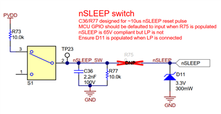
I have a question regarding the nSLEEP pin of the DRV8328 gate driver. From my understanding this pin can be used to put the device in sleep mode and to reset fault conditions without entering sleep mode when a low pulse is provided. I've actually found an evaluation board (see DRV8328AEVM) where this device is used. The snapshot below shows the circuitry for the nSLEEP pin in the evaluation board. nSLEEP goes straight into the MCU GPIO however it's not clear to me what happens if R75 is populated. It looks like switch S1 can be used to generate the pulse, however it's not clear to me if nSLEEP should still be connected to the GPIO of the MCU or not. 

thanks

Giorgio

  • Hi Giorgio, 

    Thanks for reaching out via the e2e forum - please see my answer below and let me know if it resolves your question.

    1. nSLEEP pin is 'active low' - meaning if you pull it low towards 0V, the device will be put into a low-power-consumption SLEEP mode 
      1. this pin is typically driven by a GPIO from the MCU to toggle the device in/out of sleep mode, but the MCU can probably only operate on logic-level voltage (<5V)
      2. that's why there's a 3.3V clamping diode to limit what voltage the MCU sees 
    2. Alternatively, it is possible to just drive the nSLEEP pin high or low with an external switch (like in your diagram) 
      1. the pin is rated for 65V abs max, so this gives you more options than just the MCU to drive the pin High
      2. Essentially what the circuit is doing is implementing a resistor divider (btwn PVDD and GND), filtering the stepped-down voltage with a capacitor, and using that as an logic voltage to drive nSLEEP high (keeping device awake) 

    Abs max rating: this pin is rated to withstand up to 65V 

    Thanks and Best Regards, 
    Andrew 

  • Hi andrew and thank you for the answer.

    So, it is either an external switch or a GPIO from the MCU, not both, right? what confused me was the comment in red that says ' MCU GPIO should be defaulted to input when R75 is populated ' which I interpreted as to connect the MCU GPIO to nSLEEP when R75 is populated. 

    How do you generate the pulse with the switch? do you have to move it from position 3 to 1 and then immediately back to 3? 

  • Hi Giorgio, 

    Attached updated response below. Let us know if this answers your question, Thanks! 

    So the main success metric here for your design implementation will be to answer the question of: 'Can I successfully toggle the voltage on the nSLEEP pin High and Low?' 

    If R75 is connected,

    • Switch toggle H/L control: nSLEEP pin can be pulled up to 'logic high' voltage through the S1 physical 'switch' on the EVM when switch is in position 3, or it can be pulled low through IC-internal pulldown resistor if the physical switch is set to position 1
      • I linked the datasheet section describing the H->L->H pulse on nSLEEP pin to achieve a reset. However, I am not sure if the EVM is meant to use the physical switch to achieve a reset, since having too long of a nSLEEP pulse will cause the device to just go into full shutdown
    • MCU toggle H/L control: the MCU can try to drive the nSLEEP pin H/L as needed - but it might get overpowered by the stronger pullup/pulldown of the external switch circuit. Having MCU retain priority here would be a matter of having weaker physical pullup/pulldown resistors or having a really powerful MCU GPIO by comparison. The comment about setting your MCU GPIO as an 'input' would be so that it doesn't try to fight the external switch's pull-up or pull-down. 

    If R75 is not connected, then 

    • Switch toggle H/L control: the switch is disconnected since you removed the R75 0-Ohm resistor path. Can't use physical switch to toggle nSLEEP. 
    • MCU toggle H/L control: the nSLEEP pin can be driven solely by the MCU's GPIO Output.

    nSLEEP physical switch (S1) can toggle the voltage high or low that ends up on the nSLEEP pin. 

    nSLEEP passive pulldown internally will keep nSLEEP=0V if there's not a stronger pull-up externally

    nSLEEP RESET Pulse procedure: 

    Best Regards, 
    Andrew 

  • Hi Andrew, thank you! this helps a lot.

    One last thing I'd like to understand better, how do you actually generate the reset pulse? The red comment in the schematic says 'C36/R77 designed for 10us nSLEEP reset pulse'. Is this the way I should follow or do you have a better recommendation to generate the reset pulse? 

  • Hi Giorgio, 

    I discussed this further with our team members, and also ran a quick experiment in the lab to assess the functionality of this switch circuit.

    • Based on our results, the labeling in the EVM schematic may be worded wrongly -> and we will work to update it in the future to avoid confusion. 
    • the actual intention of the C36/R77 components is to help reduce the signal bounce from the physical switch toggle, so that you get a smoother waveform w/ less harsh voltage transients. 


    In order to generate a RESET pulse on the nSLEEP pin, our recommendation is to use the MCU GPIO resource to drive the nSLEEP pin H->L->H within a controlled amount of time, as described by the datasheet. 

    • For best results when using the MCU, we'd suggest to DNI R75 so that the external switch circuit doesn't affect your nSLEEP pin pull-up/pull-down stronger than your MCU drive capability 

    Please help mark this thread resolved, if it answered your question. Thanks!

    Best Regards, 
    Andrew