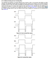
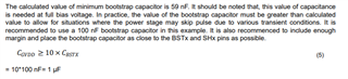
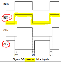
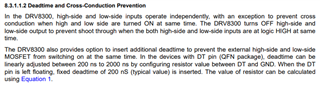
This thread has been locked.

If you have a related question, please click the "Ask a related question" button in the top right corner. The newly created question will be automatically linked to this question.

DRV8300: Bootstraping design verification

Part Number: DRV8300

Hi,

I have designed a testing circuit for an ESC. This circuit does not work. Since I am new to the design I have doubts about why it was not working. The input ports are connected to an ESP32 running on PWM at 10kHz.

I have attached the schematics, please verify and feel free for any kind of inputs or suggestions.

  • Hi Thien, 

    Please help share the requested info, and let us know if the problem gets resolved from the suggestions below. Thanks!

    some things to consider

    1. can we get some waveforms of GVDD, SHx, BSTx? 
    2. can we get some waveforms of INHx, INLx, GHx, GLx? 
    3. the device variant you are using is
      1. PW-package (no MODE pin for invert/non-invert) 
      2. no integrated diode (so it's good that you have ext diode, but will want to check against any recommendations inside datasheet
      3. inverting version part number (see datasheet section below)
        1. my suggestion is to toggle these slowly according to the commutation logic and make sure your inputs make sense for the expected outputs 
    4. bootstrap cap selection 
      1. refer to datasheet section '9.2.2 Bootstrap Capacitor and GVDD Capacitor Selection'
      2. your GVDD capacitor may be too small compared to your bootstrap caps. 
      3. the impact of this may show up in your waveforms, and the explanation for this is also in the same datasheet section 

    Best Regards, 
    Andrew 

  • Hi,

    thank you for your response.

    GVDD is connected to a 12V DC source.

    you can find the requested images here:

    https://imgur.com/a/d9bHW1A

    I am using the TSSOP version without bootstrap diode.

    Regards,

    Thien

  • Hi Thien, 

    Looking at the waveforms, I think your INLx inputs might be wrong for your device variant. 

    • You are using the DRV8300NIPWR variant, where the "I" stands for 'INVERTED' inputs (INLx=L means GLx=H)
      • see waveform below from the datasheet
      • and see below explanation of cross-conduction protection (also known as shoot-through protection) 
    • please update the input waveforms to more closely match the diagram, and let us know if results improve
      • hopefully this resolves the problems observed

    Also, you may still want to update the capacitors according to guidelines for GVDD cap and BSTx cap I described above. 

    • The datasheet will indicate the guidelines to do this

    Datasheet sections mentioned above: 

    Best Regards, 
    Andrew 

  • Thank you for your response.

    I reversed the INLx signals, however only channel A is working.

    Please find bellow the waveform of VGS HC and VGS LC

  • Hi Thien, 

    Can you share a waveform of INHx, INLx, GHx, GLx on the same scope capture? 

    We need to check that the commutation logic is correct 

    Best Regards, 
    Andrew 

  • Hi,

    please find the required info in the link

    https://imgur.com/a/2DuCFuR

    Regards,

    Thien

  • HI Thien,

    Your PWM inputs look okay, it looks like your gate drive outputs do not have enough gate drive current (IGVDD) to switch the high side gate outputs (GHA, GHB, and GHC).  

    This could be due to a few issues:

    - Too small of GVDD bypass capacitance (recommend 10uF, not 4.7uF)
    - Not enough current supply from GVDD source (ideally should provide at least 50mA average current). You should calculate it based on this equation:


    Could you increase the GVDD cap to 10uF to see if this improves performance? 

    Can you share layout of your PCB?

    Thanks,
    Aaron