This thread has been locked.

If you have a related question, please click the "Ask a related question" button in the top right corner. The newly created question will be automatically linked to this question.

BOOSTXL-DRV8323RS: I can't get the DRV8323RS to talk SPI to either the F280049 or the F280025 processor

Part Number: BOOSTXL-DRV8323RS
Other Parts Discussed in Thread: DRV8323, SYSCONFIG, LAUNCHXL-F280049C

I connected an F280049C Launchpad to a BOOSTXL-DRV8323RS and the SPI communication will not work.  
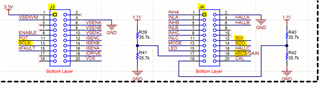
My connections:

I used jumpers to connect the following pins: (only these connections are made -- no others)

Signal GPIO F280049 pin DRV8323
3.3v J1-1 J3-1
GND J3-22 J3-4
ENABLE GPIO-13 J1-3 ENABLE J3-9
SCLK GPIO-22 J5-47 SCLK J3-13
SIMO GPIO-30 J4-33 SDI J4-12
SOMI GPIO-57 J2-19 SDO J4-14
STE GPIO-40 J1-4 nSCS J4-18

I tried simple code that did not work and then I copied code from the universal motorcontrol lab example for the F280025 processor which has many more waits and checks but neither works.

The following code was generated by sysconfig:

#define GPIO_PIN_SPIB_SIMO 30
#define GPIO_PIN_SPIB_SOMI 57
#define GPIO_PIN_SPIB_CLK 22

#define ENABLE 13
#define CS_PIN 40

#define mySPI0_BASE SPIB_BASE
#define mySPI0_BITRATE 1000000

#include "board.h"

void Board_init()
{
	EALLOW;

	PinMux_init();
	GPIO_init();
	SPI_init();

	EDIS;
}

void PinMux_init()
{
	//GPIO13 -> ENABLE Pinmux
	GPIO_setPinConfig(GPIO_13_GPIO13);
	//GPIO40 -> CS_PIN Pinmux
	GPIO_setPinConfig(GPIO_40_GPIO40);
	//SPIB -> mySPI0 Pinmux
	GPIO_setPinConfig(GPIO_30_SPIB_SIMO);
	GPIO_setPinConfig(GPIO_57_SPIB_SOMI);
	GPIO_setPinConfig(GPIO_22_SPIB_CLK);

}

void GPIO_init(){
		
	//ENABLE initialization
	GPIO_setDirectionMode(ENABLE, GPIO_DIR_MODE_OUT);
	GPIO_setPadConfig(ENABLE, GPIO_PIN_TYPE_PULLUP);
	GPIO_setMasterCore(ENABLE, GPIO_CORE_CPU1);
	GPIO_setQualificationMode(ENABLE, GPIO_QUAL_ASYNC);
		
	//CS_PIN initialization
	GPIO_setDirectionMode(CS_PIN, GPIO_DIR_MODE_OUT);
	GPIO_setPadConfig(CS_PIN, GPIO_PIN_TYPE_PULLUP);
	GPIO_setMasterCore(CS_PIN, GPIO_CORE_CPU1);
	GPIO_setQualificationMode(CS_PIN, GPIO_QUAL_ASYNC);
}
void SPI_init()
{
	
	//mySPI0 initialization
	SPI_disableModule(mySPI0_BASE);
	SPI_setConfig(mySPI0_BASE, DEVICE_LSPCLK_FREQ, SPI_PROT_POL0PHA0,
				  SPI_MODE_MASTER, 1000000, 	16);
	SPI_disableFIFO(mySPI0_BASE);
	SPI_disableLoopback(mySPI0_BASE);
	SPI_setEmulationMode(mySPI0_BASE, SPI_EMULATION_STOP_AFTER_TRANSMIT);
	SPI_enableModule(mySPI0_BASE);
}

I then setup my main code based on the driver lib SPI example:

#define CS_PIN_B      40
#define CS_LOW_B                      GPIO_writePin(CS_PIN_B, 0)
#define CS_HIGH_B                     GPIO_writePin(CS_PIN_B, 1)


void main(void)
{
    uint16_t sData = 0x8000;                  // Send data
    uint16_t rData = 0;                  // Receive data
    volatile SPI_RxFIFOLevel RxFifoCnt = SPI_FIFO_RXEMPTY;
    uint16_t n;
    volatile uint16_t WaitTimeOut = 0;
    bool rxTimeOut;


    //
    // Initialize device clock and peripherals
    //
    Device_init();

    //
    // Disable pin locks and enable internal pullups.
    //
    Device_initGPIO();

    //
    // Initialize PIE and clear PIE registers. Disables CPU interrupts.
    //
    Interrupt_initModule();

    //
    // Initialize the PIE vector table with pointers to the shell Interrupt
    // Service Routines (ISR).
    //
    Interrupt_initVectorTable();

    //
    // Board initialization
    //
    Board_init();
    GPIO_setPadConfig(DEVICE_GPIO_PIN_SPISIMOB,GPIO_PIN_TYPE_PULLUP);
    GPIO_setQualificationMode(DEVICE_GPIO_PIN_SPISIMOB,GPIO_QUAL_ASYNC);

    GPIO_setPadConfig(DEVICE_GPIO_PIN_SPICLKB,GPIO_PIN_TYPE_PULLUP);
    GPIO_setQualificationMode(DEVICE_GPIO_PIN_SPICLKB,GPIO_QUAL_ASYNC);

    GPIO_setPadConfig(DEVICE_GPIO_PIN_SPISOMIB,GPIO_PIN_TYPE_PULLUP);
    GPIO_setQualificationMode(DEVICE_GPIO_PIN_SPISOMIB,GPIO_QUAL_ASYNC);

    // Must put SPI into reset before configuring it
    SPI_disableModule(mySPI0_BASE);

    // SPI configuration. Use a 500kHz SPICLK and 16-bit word size, 25MHz LSPCLK
    SPI_setConfig(mySPI0_BASE, DEVICE_LSPCLK_FREQ, SPI_PROT_POL0PHA0,
                  SPI_MODE_MASTER, 400000, 16);

    SPI_disableLoopback(mySPI0_BASE);

    SPI_setEmulationMode(mySPI0_BASE, SPI_EMULATION_FREE_RUN);

    SPI_enableFIFO(mySPI0_BASE);
    SPI_setTxFifoTransmitDelay(mySPI0_BASE, 0x10);

    SPI_clearInterruptStatus(mySPI0_BASE, SPI_INT_TXFF);

    // Configuration complete. Enable the module.
    SPI_enableModule(mySPI0_BASE);

    CS_HIGH_B;

    GPIO_writePin(ENABLE, 1);
    GPIO_writePin(ENABLE, 1);

    DEVICE_DELAY_US(100000L);

    //
    // Enable Global Interrupt (INTM) and realtime interrupt (DBGM)
    //
    EINT;
    ERTM;

    //
    // Loop forever. Suspend or place breakpoints to observe the buffers.
    //
    while(1)
    {
        CS_LOW_B;
        CS_LOW_B;

    // wait for registers to update
    for(n = 0; n < 0x08; n++)
    {
        __asm(" NOP");
    }

    // reset the Rx fifo pointer to zero
    SPI_resetRxFIFO(mySPI0_BASE);
    SPI_enableFIFO(mySPI0_BASE);

    // wait for registers to update
    for(n = 0; n < 0x20; n++)
    {
        __asm(" NOP");
    }

    // write the command
    SPI_writeDataBlockingNonFIFO(mySPI0_BASE, sData);

    // wait for two words to populate the RX fifo, or a wait timeout will occur
    while(RxFifoCnt < SPI_FIFO_RX1)
    {
        RxFifoCnt = SPI_getRxFIFOStatus(mySPI0_BASE);

        if(++WaitTimeOut > 0xfffe)
        {
            rxTimeOut = true;
        }
    }

    WaitTimeOut = 0xffff;

    // wait for registers to update
    for(n = 0; n < 0x200; n++)
    {
        __asm(" NOP");
    }

    CS_HIGH_B;
    CS_HIGH_B;

    // Read the word
    rData = SPI_readDataNonBlocking(mySPI0_BASE);


    if (sData == 0x8000){
        sData = 0xB000;
    }else sData = 0x8000;
        DEVICE_DELAY_US(500L);
    }
}

I hooked up a Saleae to the pins and get this from the code.  No matter what I try, I ALWAYS get 0000 back on the SDO line. This makes no sense.  I tried all different registers and tried a variety of delays and timing changes.

As far as I can tell, the ENABLE is enabled, and the clock and input to the DRV8323 looks correct, but I never get a response.  Is there something else I need to do to the chip to get it to listen and respond?

Regards,

Neil

  • Hi Neil,

    Thank you for posting your question on the motor drives forum! Can you ensure that the ENABLE signal of the device is held high during this test?The STE/nSCS needs to be pulled low during SPI communication, but the ENABLE signal needs to be held high during the SPI communication since ENABLE is the signal that is used to enable the DRV or put the DRV into sleep mode.

    Regards,

    Anthony Lodi

  • Anthony,

    Thank you for the help.  The enable line is pulled high at the start of the program and left high throughout.  I just tried to change the software so that its the opposite of what you suggest -- ENABLE is low instead of high, in this case, the SDO signal is always high 0xFFFF instead of the 0x0000 shown above in the code as posted.  Any other suggestions?

    Regards,

    Neil

  • What about pull up or pull down resistors?  I do not have them currently on any of the signals but I tried pull-ups on the SDO but it made no difference.  I set the '049 processor to use internal pull-ups on all the GPIO lines used for SPI, however, I do not know if that actually does anything if the GPIO is used for SPI.

  • Hi Neil,

    Let me get back to you on this next week.

    Regards,

    Anthony Lodi

  • Hi Neil,

    A pullup resistor is necessary on the SDO line, but the other SPI lines do not need any pullup or pulldown resistors. For the SDO line a 1k-10k ohm resistor should be fine. 

    Could you hook up the Saleae to all 4 SPI lines and zoom in to show 1 a single read command from the MCU to the DRV of register 0x03? I want to analyze the waveform to see if there is anything that is incorrect.

    Regards,

    Anthony Lodi

  • Anthony,

    I added the pull-up resistor on SDO (which is the green MISO channel below.  I verified it with a voltmeter that pin sits at 3.3v when not in use and the Saleae measures it as high when unclocked and low when clocked. Here is a read command for DRV register 0x03.  The word is 0x03 << 11 + 0x8000 for the read bit = 0x9800\

  • Hi Neil,

    Thanks for the waveforms! Based on what you have provided, assuming that those lines that you probed are properly connected to the correct SPI pins of the DRV, I don't see any issue with the SPI command that is being sent to the DRV8323 device. The BOOSTXL-DRV8323Rx board is a modifiable board to support both SPI and hardware variants, so I want to make sure that there hasn't been any component depopulated (or populated) that could be disconnecting the SPI lines from the actual device. Could you confirm the following:

    1. R13, R15, and R17 are populated with 0 ohm resistors

    2. R14, R1, R5, R16, R19, and R22 are depopulated

    3. The chip select signal is connected to pin 18 of J4, the SDO signal is connected to pin 14 of J4, the SDI signal is connected to pin 12 of J4, and SCLK is connected to pin 13 of J3 as shown below? Note: Figure 4 of the users guide accidentally labels both pins 13 and 15 of J3 as SCLK. Only pin 13 is SCLK, pin 15 is nFAULT, not SCLK.


    Regards,

    Anthony Lodi

  • Anthony,

    The DRV board is new, unmodified out of the box but to confirm:

    1. R13, R15, and R17 are populated with 0 ohm resistors.

    -- double checked 

    2. R14, R1, R5, R16, R19, and R22 are depopulated

    -- double checked

    3. The chip select signal is connected to pin 18 of J4, the SDO signal is connected to pin 14 of J4, the SDI signal is connected to pin 12 of J4, and SCLK is connected to pin 13 of J3 as shown below? Note: Figure 4 of the users guide accidentally labels both pins 13 and 15 of J3 as SCLK. Only pin 13 is SCLK, pin 15 is nFAULT, not SCLK.

    yes.  Please see the connection chart in my initial post.  It agrees with your DRV connections (although you can look on that chart to see if I made any mistakes on the '049 processor side.)  All those connections were made with one addition of the pull-up resistor on SDO to 3.3v with a 1.5 kohm resistor.  I have tried multiple boards so it does not seem to be hardware damage.

    Thank you for looking into this.

    Regards

  • Hi Neil,

    Thanks for confirming! 

    Could you disconnect the SDO line from the LAUNCHXL-F280049C and perform the same test of hooking up the Saleae to all 4 SPI lines on the BOOSTXL-DRV8323RS and zoom in to show a single read command from the MCU to the DRV of register 0x03? The purpose of this test is to rule out the possibility of something on the LAUNCHXL-F280049C pulling down the SDO line which is causing it to not be able to pull up the line during a SPI read. 

    Could you also measure the VM voltage on the BOOSTXL-DRV8323RS during this test to make sure that the device is powered up? Another way to tell that the device is properly powered up is to probe the C8 capacitor on the pad nearest to the device to see if it shows about 3.3V (this is the DVDD output). 

    If there are no issues seen with the previous tests, you can perform a SPI read of register 0x03 while probing the SPI lines on R13 (SDO), R15 (SDI), R17 (SCLK), and the nSCS signal. Probing them at those points will help verify the SPI signals close to the actual device pins. 

    Regards,

    Anthony Lodi

  • Anthony,

    I got it running!  Maybe you can help me explain why.  Disconnecting the LAUNCHXL card on the SDO line did not help.  I used your second suggestion above and measured the voltage at C8 -- I was getting only 2.8V instead of 3.3V and the data sheet says it needs to be 3V minimum.  I hooked up a bus voltage of 17.5V to the VM on the BOOSTXL-DRV8323RS card, disconnected the 3.3v from the LAUNCHXL-F280049C (only keeping the grounds connected) and the C8 capacitor is now at 3.5V and it runs!!  Is the LAUNCHXL-F280049C unable to supply enough power to the BOOSTXL-DRV8323RS to run it without the external supply?  It seems odd that I could not give the chip only 3.3v and get SPI to run.

    FYI, I do not need the pull-up resistor on SDO (and I do not need to set the 0049 processor for pull-ups -- the standard configuration from Ssyconfig now works.

    Thank you for the help but now I have a bigger problem -- my embedded board does the same thing as the setup above before I supplied the external power.  I tested my EXACT embedded code on the BOOSTXL-DRV8323RS- LAUNCHXL-F280049C combination (I use the same pins) and it works on the prototype setup now.  Unfortunately, The embedded system does not work with that code so there must be a power/hardware problem.  I checked C8 (which is C82 on my board -- see below) and it has 3.5V on the embedded DRV. All the connections to the DRV should be the exact same as the Launchpad setup (which is why I jumped to the Launchpad to do the test.). Here is my circuit using the 40pin DRV chip.  Can you see why the embedded version fails while the Launchpad version works?  Can you direct me to do some measurements which might point to the problem?

    Regards

  • Hi Neil,


    Great to hear that you were able to get the SPI communication to work!

    The typical value for the VM undervoltage lockout threshold for the DRV8323 is 5.6V for VM falling and 5.8V for VM rising, so the 3.3V from the launchpad is insufficient to power the device properly. The DVDD LDO is generated from VM, and DVDD is used to power the internal digital logic. Applying a 6V or greater voltage to VM will allow you to properly communicate with the device. 

    You mentioned that you do not need a pullup on SDO, however the device actually does need one because SDO is an open drain output. The EVM already has a pullup on the SDO line already (R12), so if that is populated then you shouldn't need any additional external pullup. 

    Regarding the issue of the embedded board not working, it is likely due to the fact that SDO is an open drain output and it looks like you don't have a pullup resistor on the SDO pin to pull up that line to 3.3V. Additionally, I do not see a pullup resistor on nFAULT. nFAULT is an open drain output, and therefore requires an external pullup. 

    I would recommend adding some bulk capacitance of 10uF or greater to VM in order to provide a more stable VM supply for longer transients.

    Regards,

    Anthony Lodi 

  • The pull-up resistor did the trick.  I did not notice that on the Boostxl schematic.  

    Regards

    Neil

  • Hi Neil,

    Glad to hear that you were able to resolve the issue with the pull-up resistor on nFAULT!

    Regards,

    Anthony Lodi