Hello,
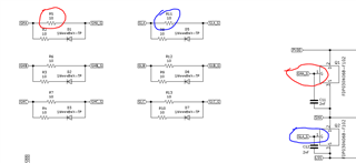
I'm assembling the PCB for a 1kW inverter that I've designed for a BLDC motor application. I got to the stage where I've just hand soldered the gate driver DRV8328ARUYR and I would like to test it on its own to make sure I've properly soldered all the pins to the pads and I've not damaged the device (I used a heat gun to do the soldering) before soldering the MOSFETs devices on the power stage and the MCU. The components I soldered are represented in the schematic below:
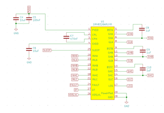
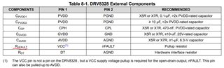
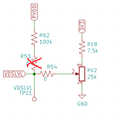
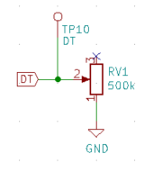
where PVDD is the main supply (36V); SPEEP, INHA, INLA, INHB, INLB, INHC, INLC and FAULT are routed directly the TMS320F28034PNS uC; DT and VDSLVL are connected to 2 POTs (see snapshots below); GHA, GLA, GHB, GLB, GHC, GLC are routed to the MOSFETs gates through the external gate resistance; SHA, SHB, SHC are routed to the sources of the high side MOSFETs and LSS is routed to the sources of the low side MOSFETs.
First of all, could you please confirm that the above configuration is correct?
Do you think I can test the DRV8328ARUYR device with only the surrounding caps installed?
The way I was thinking of testing it was to supply the device with 36V at the PVDD pin, then provide 3.3V to the SLEEP pin to awake the device and apply 3.3V to one of the gate drive input (INHx or INLx). Then, I would measure the voltage at the corresponding output (GHx or GLx). Do you think I can do that? Do you have any feedback on how to test it?
thanks
Giorgio