This thread has been locked.

If you have a related question, please click the "Ask a related question" button in the top right corner. The newly created question will be automatically linked to this question.

DRV8305-Q1: Noise on AmplifierOutput coincident to chargepump activity

Part Number: DRV8305-Q1
Other Parts Discussed in Thread: DRV8305

Hello,

I'm using the DRV8305NQ within a 24V / 350W BLDC motor electronics prototype. 

The motor control is based on F280049 and instaspin FOC software.

The implementation is close to the DRV8305 evaluation board.

Basically the system is working as intended, but there is an issue concerning the quality of incoming phase current signals.

Monitoring the phase current signals by application software shows, that there are short disturbances with amplitudes up to 2A,

even if the powerstage is not switching.  According instaspin FOC software, the signals are sampled in the middle of the lowside-FET ON-time,

i.e. there are no switching events in a certain time-span around the sample point. All three motor-phase-current-signals are sampled simultaneously,

each by one of the three ADC units of the F280049 controller.


The disturbance effects mostly all three signals at the same time.

The impact on signal Ia is least, on signal Ic most. 

The amplitudes of the disturbances are rising by increasing the PVDD supply voltage (e.g. from 10V.....32V).  

I could find a correlation between the disturbances and the operation of the chargepump of the DRV8305. 

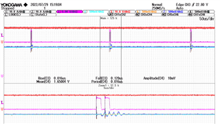
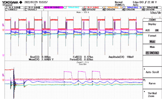
Pink: voltage at chargepump 'flying' capacitor CP2H

Blue: phase current signal 

Red: phase voltage (const., no switching)

system without motor operation (no switching):

system with motor in operation:

The chargepump pulses (i.e. disturbances) are asynchron to the motor PWM switching and are drifting again and again into the ADC sample point. 

As background information : the phase current signal configuration is:

2mOhms shunt in the 'foot' of the half-bridge

amplification (DRV8305 amplifier) x20,    (with offset 1,65V, i.e. 0A = 1,65V)

resulting in 40mV/A    

On basis of  3,3V signal range, the theoretical current range is +/-41,25A

Using a 12bit  AD-converter, the resolution is about 20mA/lsb

Is the obeyed effect basically known ?

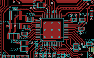
Up to now, I couldn't detect the effect on DRV8305 EVM. I suppose, this is due optimized layout. 

The layout of our prototype hardware is mostly close to the EVM, but maybe not optimal.

Is there a possibilty to check some aspects of our design ?  


How can I weaken the effect of chargepump influencing the measurement ?

note#1 : as a trial, I add a 12 Ohm series resistor in the current path of each flying 47nF capacitor, what effects a significant lower disturbance.

However, this is not acc. application note/ not intended for final design.

note#2: connecting the scope-probe (or a short piece of wire) on CPH2 had an effect on disturbance amplitude ! 

Friendly Regards 

Martin Bayer        

  • Hey Martin,

    Thank you for posting your question on the E2E. I will consult with the team and aim to provide feedback by middle of next week.

    I would like to review the schematic and layout to help debug the situation. Would you be able to provide a pdf of them?

    Also what is the rating of the 47nF CP2H capacitor?

    Best Regards,

    Akshay

  • Hello,

    thank you for your review offer, enclosed the needed files 

    A134A04pdf.zip

    The charge pump flying capacitors have following key-spec.:

    In general, all supporting capacitors 'around' the DRV8305 are choosen as MLCC -type.

    Friendly regards

    Martin Bayer

  • Hey Martin,

    Thank you for providing the necessary documents.

    I will review with the team and aim to provide feedback next week.

    Best Regards,

    Akshay

  • Hey Martin,


    What voltage were these disturbances captured at? Are these disturbances unacceptable at 10V?


    Could you isolate the CSA layers, I want to see if they go near the charge pump capacitors, CP1H and CP2H? It might be possible that some noise is being coupled to the CSA.


    I believe the voltage rating of these capacitors are not high enough. Would it be possible to have CP2H capacitor be higher voltage rated? Our EVM uses 100V rated caps for CP2H and 50V rated caps for CP1H. Also what is the voltage rating of your VCPH?


    Do you have thermal vias in your design?


    Best Regards,

    Akshay

  • Hello Akshay,

    thanks for your input,

    I started several trials to optimize the signal quality, but in the end I couldn't achieve a big improvement in scope of the existing pcb design.

    At first to your questions:

    If analyzing the signal quality by monitoring the ADC conversion results (DRV8305 interfaced with a F280049), the basic noise is in a range of about 10lsb. Regarding a  fullscale  range of +/-41A and resolution of ~20mA/lsb this is acceptable (<0,05%). The disturbances apeare in terms of  'spikes' with  amplitudes up to 2A, this is more than 5% of measurement range. The spikes vary in amplitude and frequency of occurence.

    At 10V supply (PVDD) the disturbances do not take effect.

    I seems nearly so, that there would be a treshold or something like that at above 10V. Increasing PVDD above that level, results in starting 'disturbance generation'. Amplitudes increase with increasing PVDD. Our nominal target operation voltage is 24V (18..32V).

    Conc. CSA layers routing its slightly laborious to provide an overview, but I checked if there may be a critical mixture of chargepump and CSA PCB-resources. From my opinion there is a clear seperation of areas, tracks and layers used for chargepump and for CSA.

    For checking the possible MLCC derating effect, I assembled CPH2 capacitor with a 100V type.  Unfortunately without a remarkable effect.

    Vias (9x) to the ground layers are supported below the thermal pad of the DRV8305.

    The good news are, if using the TI-DRV8305EVM with an F280049 launchpad, I could not observe any disturbances on the phase current signal lines.

    From schematic view, our electronics design is very close to the DRV8305EVM and the application note. A remarkable difference is the circuit from DRV8305 OPamp-out to F280049 ADC-In: In DRV8305EVM there is designed a RC-circuit using a series resistor (56R) and a capacitor (2nF). Our design supports only a 100pF capacitor close to the ADC-Input in the signal line. Experimental adding the RC-circuit to our design shows a small improvement, but did not suppress the obeyed effect in general.

    From pcb-layout view, the EVM is optimal designed. In comparision I would judge, that our design is not optimal conc. blocking caps. I did some trials to optimize the critical tracks with small success in view to lower disturbances, however I never achieved the signal quality of the EVM.

    I also assembled the EVM with the chargepump capacitors, used by our electronics, without effect. 

    Although the root cause is not clear for me, I hope that by reworking the pcb layout in view to connecting blocking capacitors the issue can be fixed.

    Friendly regards

    Martin          

  • Hey Martin,

    Thanks for the feedback. Please let me know if you get any additional information from reworking PCB layout.

    Best Regards,

    Akshay