This thread has been locked.

If you have a related question, please click the "Ask a related question" button in the top right corner. The newly created question will be automatically linked to this question.

DRV8323: DRV8323HR

Part Number: DRV8323

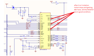
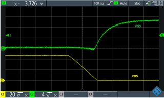
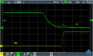
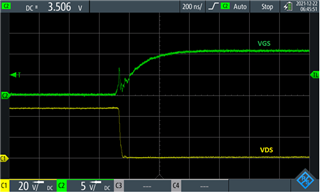
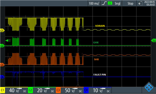
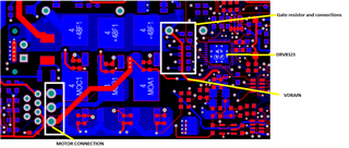
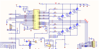
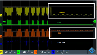
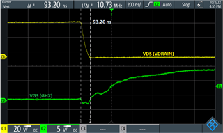
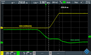
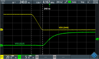
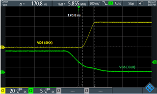
we are encountering a problem with DRV8323HR. The motor is about start but it stops after 2 or 3 seconds.

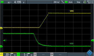
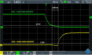
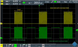
we probed the pins and noticed that , voltage at highside MOSFET drain and source pins are same (48v ie  Vcc). and drv fault is getting . could you please help us to debug the issue??

  • Hey Balabhaskar,

    I will look more into the issue and aim to provide feedback by Wednesday next week.

    Best Regards,

    Akshay

  • Thank you Akshay! Please let us know if any further details required. Please see below image for your reference. 

  • Hey Balabhaskar,


    What IDrive setting are you using? It might be possible that too high of an IDRIVE is causing a short.

    Is there a pullup resistor on nFAULT to VCC?


    Could you provide a waveform of VDRAIN, GHx, SHX, and nFAULT as this might help debug this issue?


    Best Regards,

    Akshay

  • What IDrive setting are you using? 120mA source current and 240mA sink current.

    Is there a pullup resistor on nFAULT to VCC? Yes, pulled up to 5V through 10K resistor

    Could you provide a waveform of VDRAIN, GHx, SHX, and nFAULT? Wave forms are captured before DRV 8323 damage below. 

    Turn on—Low-Side MOSFET  VGS and VDS

    Turnoff—Low-Side MOSFET   VGS and VDS

    Turnon—High-Side MOSFET   VGS and VDS

    Turnoff—High-Side MOSFET   VGS and VDS

    Dead time 

    PWM signal for high side and low side MOSFET

  • Hi Akshay,

    Please find my comment below

    Could you provide a waveform of VDRAIN, GHx, SHX, and nFAULT? waveforms captured for damaged DRV8323 while rotating 2or 3 revolutions below and please let us know if any further details required.

  • Hey Balabhaskar,

    Thank your for providing the waveforms. I will consult with the team and aim to provide feedback before the end of day Friday.

    Best Regards,

    Akshay

  • We are waiting for your valuable feedback, could you please check and reply asap?

  • Hey Balabhaskar,


    This device has a maximum operational voltage of 60V and 48V is very high so the layout must be very well designed in order to mitigate the effect of parasitics.


    Are you using the VDS OCP? If so what is your trip setting?


    It is very possible that the Idrive setting used is very high. Would it be possible to reduce the IDrive setting to see if it helps with the issue? VDS might be coupling into the low side and lower Idrive might help with this.


    Could you share your layout and schematic in order to help assess the design?


    I also wanted to clarify what you meant by damaged drv8323. What part is damaged?


    Best Regards,

    Akshay

  • Hi Akshay,

    Thank you for your comments, please find my comments below.

    Are you using the VDS OCP? If so what is your trip setting? Yes, tripping setting is at 11.5A rms

    It is very possible that the Idrive setting used is very high. Would it be possible to reduce the IDrive setting to see if it helps with the issue? VDS might be coupling into the low side and lower Idrive might help with this. Ok will try this but current Idrive is 120mA source and 240mA sink, and rise time and fall time we are getting below

    Highside Turn ON             :-300ns

    Highside Turn OFF            :-300ns

    Lowside Turn ON              :-220ns

    Lowside Turn OFF            :-220ns

    Could you share your layout and schematic in order to help assess the design?

    please let us know if any further details required.

    thanks 

  • Hey Balabhaskar,

    Thank you for providing additional information. I will aim to provide feedback before the end of the week. 

    Best Regards,

    Akshay

  • Thank you Akshay, Could you please consider it as a high priority? 

  • Hey Balabhaskar,


    1)The schematic is blurry and I can’t read part values, so could you please upload a pdf version?


    2) I am still not sure on the damage you mentioned. What do you mean by damaged, which specific part? Is there a short or a burn?

    3) An overcurrent scenario will lead to retry modes, but we see that the nfault is latched low. This suggests to me that we are seeing a gate driver fault. If the device is operational and not damaged then I would like to see if the latched fault always occurs. If it does then it might suggest that there is a short/damage causing the nfault to be low.

    4) If there is damage then we can perform impedance check on the pins to narrow down where the short has occurred.


    Best Regards,

    Akshay

  • Hi Akshay,

    Please find my comments below.

    1)The schematic is blurry and I can’t read part values, so could you please upload a pdf version? uploaded


    2) I am still not sure on the damage you mentioned. What do you mean by damaged, which specific part? Is there a short or a burn? I am not observed any short or burn but after 2 or 3 rotation I noticed that VDRAIN pin goes low and SHX pin goes high. After removing all high side MOSFET, still I observed 48V on SHX pin.

    3) An overcurrent scenario will lead to retry modes, but we see that the nfault is latched low. This suggests to me that we are seeing a gate driver fault. If the device is operational and not damaged then I would like to see if the latched fault always occurs. If it does then it might suggest that there is a short/damage causing the nfault to be low. Latched fault always occurs, after power cycle we can able to run 2 or 3 rotations then latched fault occurs.

    4) If there is damage then we can perform impedance check on the pins to narrow down where the short has occurred. I will remove the IC and test it one more time and update you

    05.ROLL1.pdf

  • Hi Akshay,

    Could you please  check the layout and suggest if any improvement is required? Is it possible to have a session on a teams meeting to check the layout with you ?

  • Hey Balabhaskar,

    Thank you for the additional information. I will perform a schematic review and aim to provide feedback by the middle of next week.

    Best Regards,

    Akshay

  • Hi Akshey,

    Hope you are done the schematics review. Could you please provide the feedback?

  • Hey Balabhaskar,


    Please consult the schematic attached below with my comments.


    On the low side turn off waveform, I am a bit concerned seeing the ringing. The voltage goes up to 3V which is higher than your MOSFETs Vgs threshold of 1.5V. This might lead to the MOSFGET turning on every time it occurs leading to a shoot through current. If this is the root cause you can use MOSFETs with higher threshold voltage (we can keep this as a last resort).


    Also, we measure slew rate time based on VDS not VGS. So, the rise/fall time is with respect to VDS. Based on the waveform provided I see a slew rate of ~20ns which is very fast. I would recommend lowering the IDRIVE till you get a slew rate between 100-200ns. Please provide a waveform once the update has been done. The fast slew rate can lead to dv/dt coupling (gate turns on) and can lead to shoot through current. The large spikes could also lead to damage during operation. Other than lowering your Idrive setting you can also increase the dead time to combat this issue.

    Trise/fall = QGD/Isource/sink

    You could also increase gate resistance to decrease gate current.


    What was the purpose of removing the high side MOSFETs? We don’t recommend spinning the motor without the HS mosfets.


    Would it be possible to provide a zoomed in waveform of the GHx, SHx, VM and Vdrain after implementing the changes recommended?


    Best Regards,

    Akshay05.ROLL1-TI Reviewed.pdf

  • Hi Akshay,

    IDRIVE  is reduced to 30mA source and 60mA drain and gate resistance is 33 ohm , waveforms captured are below after the changes

    High side MOSFET turn on

    High side MOSFET turn off

    Low side MOSFET turn ON

    Low side MOSFET turn OFF

    waveform for VM

     Other than lowering your Idrive setting you can also increase the dead time to combat this issue. DRV8323HRTAR, there is no option to change dead time setting.

    What was the purpose of removing the high side MOSFETs? We don’t recommend spinning the motor without the HS mosfets. We are getting 48V on SHX pins after 2 or 3 rotations in the Damaged DRV, So we removed the high side MOSFETs to make sure the current path is not via the MOSFETs. But we are still getting 48V on the SHX pins after removing the  high side MOSFETS.


    Thanks,

  • Hi Akshay,

    We have reduced the gate resistance from 33 ohm to 15 ohm with IDRIVE setting 30mA source and 60mA sink, but we have observed DRV8323 failure while loading the motor. Could you please check the reason for this failure also? 

    Thanks, 

  • Hey Balabhaskar,

    Why did you decrease gate resistance? Lowering gate resistance will increase gate current.

    Just to confirm after making the change to Idrive and increasing gate resistances, did you use the old damaged board or a new one to get the waveforms? 

    Best Regards,

    Akshay

  • Hi Akshay,

    Please find my comments below.

    Why did you decrease gate resistance? Lowering gate resistance will increase gate current. We have done a iteration with 15 ohm gate resistor and 30mA Idrive  but failure observed. Then we have increased gate resistance (33 ohm ) in the new board and took all the waveforms above.  

    Just to confirm after making the change to Idrive and increasing gate resistances, did you use the old damaged board or a new one to get the waveforms? New board 

  • Hey Balabhaskar,

    Thanks for the update. I will get back to you before the end of the week.

    Best Regards,

    Akshay

  • Hey Balabhaskar,


    What resistor setting are you using for VDS_OCP? I want to know the trip voltage.

    Is the enable bit staying high for the entire duration of the operation? A waveform of enable pin and nfault would be helpful.

    Could you provide a waveform of the VDS, VGS, phase current and nfault on the same plot?

    Essentially, we need to figure out which of the following conditions are leading to the fault being observed.

    Best,

    Akshay

  • Hi Balabkhaskar, 

    Closing this thread - please let us know if you need further assistance, and help mark the answer above as 'resolved' if it answered your question. Thanks!

    Best Regards, 
    Andrew