This thread has been locked.

If you have a related question, please click the "Ask a related question" button in the top right corner. The newly created question will be automatically linked to this question.

DRV8353: Mosfet Parameter Optimization for HS and LS Switching

Part Number: DRV8353

Hi TI Forum,

We are using DRV8353 smart gate driver. We have a trouble HS and LS mosfet switching and optimization of idrive, tdead, tdrive and gate resistor.

Our used mosfet has 100ns rise and fall time with 45nC gate-to-drain charge and 150nC total gate charge, typically.

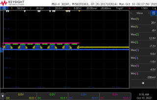
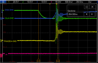
When we go with 22ohm gate resistor, there is less overshoot, undershoot and oscillation for gate and phase signals but more important HS and LS switching not correct.

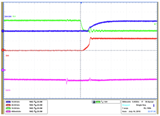
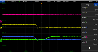
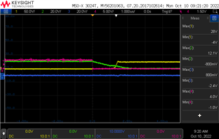
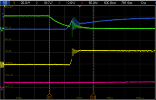
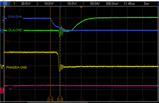
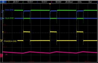
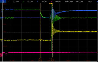
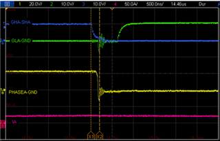
Blue=GHA-SHA Signal,Green=GLA-GND Signal, Yellow=SHA-GND Signal, Purple=Phase A Current

(Rgate=22ohm, I_drives=300/600mA, t_dead=400ns, t_drive=4000ns, 20A LOADED)


There is no affect increasing i drives for rising and falling time because of gate resistor limiting current.

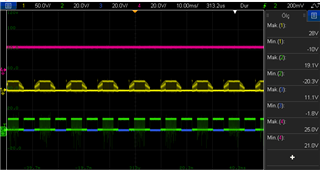
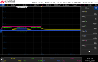
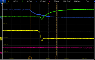
Other, if we decrease the gate resistor value to 2.7ohm, switching is correct but oscillation and other unwanted things happen at some time of switching.

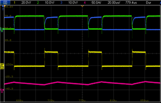
(R_gate=2.7ohm, I_drive=300/600mA, t_dead=400ns, t_drive=4000 ns, 20A LOADED)


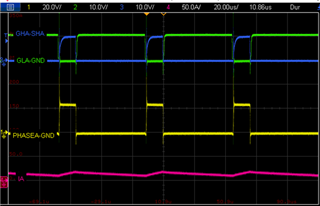
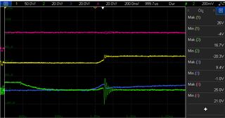
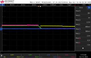
If we increase i_drive value, rising and falling times changes, but unwanted oscillations continue.

(R_gate=2.7ohm, I_drive=1000/2000mA, t_dead=400ns, t_drive=4000ns, 20A LOADED)


  • Switching loss in 22ohm state is more than 2.7ohm one. So, thermal dissipation is so much on mosfets. We should decrease it.
  • If we suddenly changed the load from 20A to 5A gate fault, overcurrent error happens in 2.7ohm gate resistor state. But, there is no error when we use 22ohm gate resistor.
  • To decrease phase voltage overshoots and others, we have done suggestions on TI App Note System Design Considerations for High-Power Motor Driver Applications. The oscillations may be occur because of tdrive and dead time.

Can you help us in this issue? How can we overcome with this signal aliasing?

Thanks in advance.

  • Hi Yardi,

    Thank you for your questions!

    You mentioned that you are targeting 100ns MOSFET rise/fall time. A few important notes: 

    1. The MOSFET rise/fall time refers to the VDS rise/fall time, not the VGS rise/fall time. So to properly understand how fast the MOSFET is switching you need to measure the VDS voltage of the MOSFETs. 

    2. A 100ns MOSFET rise/fall time is quite fast for many applications, many customers consider 200ns rise time and 100ns fall time to be a fast switching speed. 

    Proper PCB layout is critical for clean MOSFET switching. Parasitic inductance in the gate traces and the SHx traces can limit how fast you can switch a MOSFET without resulting in too much ringing on the gate and sources. From what I am gathering, you are struggling to obtain the desired MOSFET switching speed while at the same time reducing the ringing/oscillation on the gates. The solution is to either reduce the gate current/increase the gate resistance to slow down the MOSFET switching speed to reduce the ringing on the gates, or you will need to update the PCB layout to mitigate some of the parasitic inductance that is causing the ringing to occur so that you can operate at a faster switching speed without as much ringing. This can primarily be done through reducing the inductance of the gate and source traces (widening the traces to at least 20 mils width, making the distance of the traces as short as possible, and minimize the number of vias used in those paths). 

    One thing to note: increasing the gate resistor value is the same as reducing the IDRIVE current. The purpose of the gate resistor is to allow you to further tune the IDRIVE strength when the desired gate drive current is between two IDRIVE settings. As a result, a larger gate resistor will result in a slower MOSFET VDS slew rate.

    I have attached TI's Best Practices for Board Layout of Motor Drivers document. This is a great resource on various tips to implement when creating/updating the PCB layout. 

    Regards,

    Anthony Lodi

    0083.Best Practices for Board Layout of Motor Drivers.pdf

  • Hi Anthony,

    Thank you for your answer.

    Our target is not 100ns rising and falling time; it is only mosfet datasheet value.

    We think that 200ns rising and 100ns falling time is suitable for our design.

    Rising Section: 45nC/200ns=300 mA

    Falling Section: 45nC/100ns=600 mA

    If you look at our oscilloscope conditions, we have analyzed for 300/600 mA i-drive currents for source and sink.

    Other side, actually, we have carefully designed PCB section and have read this application note before the design. However, we will look at it again to check PCB design. Thank you for your suggestions.

    Actually, it is not understood that the transtion between Vgs(HS) and Vgs(LS), i mean in the switching waveform.

    (Switching waveform in DRV8353 datasheet, in our 22ohm transition above, ST AN5252 App Note Figure12)(respectively)

    In DRV8353 datasheet swiching waveform says that after Vgs(LS) totally closed, Vgs(HS) is opening. But, it is not possible to reach that by incresing gate resistor and decreasing gate drive current. Our figures are similar with the waveform in ST application note.

    Which waveform is true? What do you think about these switching waveforms?


    Thank you so much in advance.

    Regards,

    yardi

  • Hi Yardi,

    I understand your question now, thanks for the additional detail. Once the VGS voltage drops to about 2V the driver will start inserting the deadtime, and then turn on the opposite MOSFET. In this case it looks like there isn't really any deadtime between one MOSFET turning off and the opposite one turning on. I am assuming you are measuring the VGS voltage right at the MOSFET. Would you be able to take another measurement closer to the device pins? I want to see what the device is seeing vs what the driver is seeing. It may be that the VGS voltage closer to the device is less than the VGS voltage near the MOSFET due to the voltage drop across the gate resistor. This could be resulting in the driver starting the deadtime timer sooner before the voltage near the MOSFET has dropped sufficiently, leading to not enough deadtime occurring from the perspective of the MOSFET itself. 

    I would recommend to try to decrease the IDRIVE setting to lower the gate driver current instead of increasing the gate resistance up to 22 ohms. This should help achieve the similar reduction of oscillation without having to use as large of a gate resistor. The main purpose of a resistor is to further tune the gate drive strength in between two settings if necessary. 

    Regards,

    Anthony Lodi

  • Hi Anthony,

    Thank you for your support.

    We have made some tests and there is an update for the signal waveforms.

    • We have removed 22ohm and used 0ohm gate resistor.
    • 150ns falling and rising time for each. (Mosfet Qgd=45nC, 300mA/300mA source and sink current)
    • RC snubber for high side and low side gate. (Rsnub=1ohm, Csnub=33nF)
    • Vdrain-GND and Vdrain-SPA 10uF ceramic capacitor (tried up to 100uF, there is no significant difference.)
    • Gate signal traces are 20 mil, carefully designed.
    • 1PWM sync. mode is used and loaded 20A Irms.

    At the end, we have catched correct drive waveform. But, there is still a problem for low side gate signal.

    When we decrease the source current for high side mosfet (from 300mA to 150mA), gate drive fault in any phase appears. Gate signal waveform is not enough in this situation. What do you think about it? Any tdrive or dead time adjusting does not matter.

    And other, what do you suggest to improve the gate signal?


    Thank you so much.

    Best regards,

  • Hi Yardi,

    I am glad to hear that you are able to get the correct gate drive waveform! 

    You mentioned that you have an RC snubber for the high side and low side gate. I wanted to confirm that this RC snubber is not placed on the gate but rather is connected from the source to drain of each high side and low side MOSFET, correct?

    For the waveforms that you provided, which signals are measured? I am assuming that pink is VDRAIN, yellow is SHx, blue is GHx-SHx, and green is GLx to GND. Am I correct?

    When you measure the GHx to SHx voltage, are you using a single ended probe or a differential probe on the oscilloscope? 

    I am especially interested in the conditions that the device was in when the upper right waveform was taken since we see some very significant oscillations on the green waveform. What IDRIVE setting is used and what is the phase current that is flowing during this time?

    To understand more about a possible solution for the gate drive fault, would you be able to provide a waveform that is triggered on nFAULT going low and that shows the gate waveform for the gate that is triggering the fault? That will give me a better idea of what is going on at the time of the fault.

    Regards,

    Anthony Lodi

  • Hi Anthony,

    • Yes you are right, RC snubbers were located on drain-to-source of each mosfet.
    • Blue=GHA-SHA Signal, Green=GLA-GND Signal, Yellow=SHA-GND Signal, Purple=Phase A Current
    • We measured the GHA-SHA with differential probe.
    • Yes, there is a significant oscillations on the GLA-GND pin. The oscillations have decreased as much as half of upper waveform by using tip-and-barrel probe end. But, still continues.
    • Test setting: Idrives=300mA/300mA, tdrive=4000ns, tdead=100ns(or 400ns, still fault), Vds-lvl=2V, Ocp-deg= Overcurrent deglitch of 8us, Sen-lvl=sense OCP 1V. 
    • Iphase=~20A loaded.

    We will provide a waveform which you want as soon as possible.

    Thanks,

    yardi

  • Anthony,

    You can see the waveform which nFault triggered. In the last picture, Blue signal offset was adjusted 10V to see waveforms easily.

    Fault Status: 1538 or 1544

    Always VDS_OCP=1, GDF=1. Related VDS overcurrent faults on phases are changing, sometimes A, sometimes B.


  • Hi Yardi, 

    Thanks for the additional waveforms 

    Best Regards, 
    Andrew 

  • Hi Yardi,

    Thanks for the additional details!

    That makes sense that tip and barrel method reduced the oscillation seen on the low side gate signal, it could be some noise that the probe is picking up, however some of it could be due to the ringing on the source coupling in to the low side gate through the Cgd capacitance of the low side MOSFET. Here is a helpful FAQ on tuning the RC values of your snubbers: https://e2e.ti.com/support/motor-drivers-group/motor-drivers/f/motor-drivers-forum/991693/faq-proper-rc-snubber-design-for-motor-drivers

    You mentioned that the fault status was either 1538 or 1544, and that VDS_OCP and GDF are always = 1. When I convert the fault status from decimal to hex I am getting a value of 0x602 or 0x608 which would indicate FAULT bit, VDS_OCP, and either VDS_HB or VDS_HC being set (see below). In both the mentioned cases, the fault is always a VDS_OCP fault and not a GDF. If I am making a mistake in my calculations please let me know. 

    The approximate current that the VDS monitors will trip at can be calculated with the below equation:

    Itrip = VDS/Rds(on).

    You mentioned that the VDS trip level you are using is 2V. What is the Rdson value of your MOSFETs? Keep in mind that the VDS monitors for the high side MOSFETs are referenced from SHx to VDRAIN. If the VDRAIN pin is not accurately sensing the voltage across each MOSFET this could lead to the VDS monitors tripping sooner on some phases.

    Regards,

    Anthony Lodi

  • Hi again,

    When we look at datasheet, transient 200-ns low-side gate drive pin voltage (GLx) is from -5.0V to Vvgls+0.3V. With tip-and-barrel probe end, measured min. voltage and max. voltage of low side gate driver are -10.2V and +6V, respectively. It continues approximately 50ns. Is it normal or not?

    Thank you for the guide, we have used already 7-step-method to calculate the actual RC values. But, RC snubbers actually related to phase voltage ringing, SHA. As we have seen in our measurement, it does not affect GLX or GHx signal waveform so much.

    Yes, you are right about the fault status, sorry about it. In the situation that gate drive current is smaller than 300mA, we have got VDS_OCP fault. 

    How can we understand Vdrain sensing is normal or not? (typical Rds-on=4mohm, Vds=24V, 36V or 48V.)

    For 300mA high side current, everything is okay. But, if we decrease the current level to 150mA, these faults appear.

    Thank you,

    yardi

  • Hi Yardi,

    Let me get back to you on this by end of day Thursday.

    Regards,

    Anthony Lodi

  • Hi Yardi,

    My apologies for not responding sooner.

    -10.2V transients on the low side gate is concerning, I suspect that this is actually due to ringing on the low side source (which will be reflected on the gate since the gate is pulled to the source when the low side MOSFET is switched off). You could add a diode from SLx to GND along with a small resistor in the SLx path (to limit the current through the diode, as shown below) to clamp negative voltage spikes.


    Just for your information, here is another article that you may find helpful on parasitics. https://www.allaboutcircuits.com/industry-articles/understanding-and-mitigating-motor-driver-board-parasitics-through-simulation/

    Regarding the VDS monitoring, it sounds like it could be possible that the VDRAIN - SHx voltage for phases B and C are not accurately representing the drain to source voltage of those particular MOSFETs. This could be due to the placement of the VDRAIN trace relative to the drains of phase B and phase C, but one way to confirm is to measure the differential voltage from SHB to VDRAIN near the pins of the device and then measure differentially the VDS voltage of the high side FET for phase B near the MOSFET to see if it is nearing the VDS trip threshold during operation. You can repeat this for phase C as well. 

    Can you confirm which VDS trip threshold you are using?

    Regards,

    Anthony Lodi

  • Hi Anthony,

    Sorry for late response.

    Thank you for your suggestions, mayve we can use a diode from SLx to GND to protect gate driver.

    Vdrain trace is 60mil width and is going to Vbus under the 1000uF electrolytic capacitor. It is near to U phase.

    VDS_LVL is 2V, and SEN_LVL=1V. Both of them are maximum.

  • Hi Yardi,

    My thinking is that the 1000uF capacitor is holding the Vdrain voltage higher than what the actual voltage is locally near the high side drains of the V and W phases. This would be likely if the V and W phases are the farthest phases away from the 1000uF capacitor, and if the 1000uF capacitor was close to the VDRAIN pin. a 1000uF capacitor is a great help supply additional charge and maintain the supply voltage in the case of voltage dips on the battery, but the placement of the bulk capacitance in relation to the MOSFETs can be a factor in the dips that may occur locally on a particular phase. 

    You can confirm if this is the case by measuring the voltage at the drain pin of the DRV and by measuring the drain voltage right near the high side MOSFETs for phases V and W. If you see that the drain pin voltage is significantly higher than the voltage at the MOSFET drains, this could be why the VDS monitors are tripping sooner than expected.

    Changing the routing of the VDRAIN trace can help improve the VDS sensing accuracy (it would probably be best to rout it to the phase that is in the middle of the 3 phases), as well as possibly moving the 1000uF capacitor near the MOSFET drains to provide more localized bulk capacitance for the MOSFETs.

    Regards,

    Anthony Lodi

  • Hi Anthony,

    Your thinking is right, but in terms of PCB layout, it is hard to implement it.

    Actually, when we analyze DRV8353 EvKit and example layout, Vdrain goes almost to capacitor bus pin; not in the middle of 3 phases and near to A phase.


  • Hi Yardi

    Understood as to the difficulties of routing the VDRAIN trace to the middle of the MOSFETs. Another option would be to widen the polygon pours connecting  the drains together on your boards so that there is less impedance/inductance on VM to help reduce the voltage difference between the VDRAIN trace and the drains of the V and W phases. Those are the options I can suggest as solutions, if you would like me to take a look at your PCB I could give you more specific tips on how to best implement it. 

    Regards,

    Anthony Lodi

  • Hi Anthony,

    Thank you for your continuos support.

  • Hi Yardi,

    Glad I could help out!

    Regards,

    Anthony Lodi