This thread has been locked.

If you have a related question, please click the "Ask a related question" button in the top right corner. The newly created question will be automatically linked to this question.

MCT8316Z: On-chip Buck regulator failure?

Part Number: MCT8316Z

Team,

Customer is trying to debug an HW failure on MCT8316Z0TRGFR that seem to be related to the on-chip Buck regulator.
Only a small percentage of the boards are affected.
The behavior seen is as below:
-The Buck is used in inductor mode.
-The Buck outputs is outputing appr. 1V instead of the expected 5V (as programmed via pull-up on VSEL_BK pin).
-The IC shows a significant overheat compared to the one that work correctly.
I will provide more info off-line (schematics, IR pictures).

Can you please help to debug the behavior further in order to find the route cause?
Can you please review the schematics?
We have seen already the related Buck FAQ here.

Thanks in advance,

A.

  • Hi Anthony,

    I've connected with you offline to clarify some details and next steps.

    Regards,
    Eric C.

  • Dear Team,

    thanks for the help.
    The following about the questions:

    - Where exactly do you measure the 1V voltage?

    -->
    The VBK (5V) voltage on the defective module drops to approx. 0.7V
    measured here:

    --> the AVDD also have a level of only aprox. 1,7V

    - Can you provide a plot of the power up sequence for VM, AVDD and showing as well SW_BK?

    -Are the layout practice from the above FAQ  (separate ground for BK_GND and AGND directly connected or connected via a large 0-ohm R) been followed?

      --> the Grounds are not separated.

            Look the attached pdf file


    Regards,

    Michael M.

  • Hi Michael and Anthony,

    Thanks for the information! I will follow up with you in more detail over email. Please help by marking this thread as resolved.

    Best,

    Robert

  • -The Buck outputs is outputing appr. 1V instead of the expected 5V (as programmed via pull-up on VSEL_BK pin).
    -The IC shows a significant overheat compared to the one that work correctly.

    Hi,

    1) It's interesting to see the PWM signal at SW_BK pin (before the inductor).

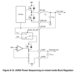
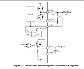
    2) AVDD regulator input is VM or Buck output? (using the buck output generates less heat on the AVDD reg.)

    Brian

  • Hello Brian,

    1) It's interesting to see the PWM signal at SW_BK pin (before the inductor).

    --> there is no PWM on a broken device. Ist only a constant voltage level of approx. 0,7V.

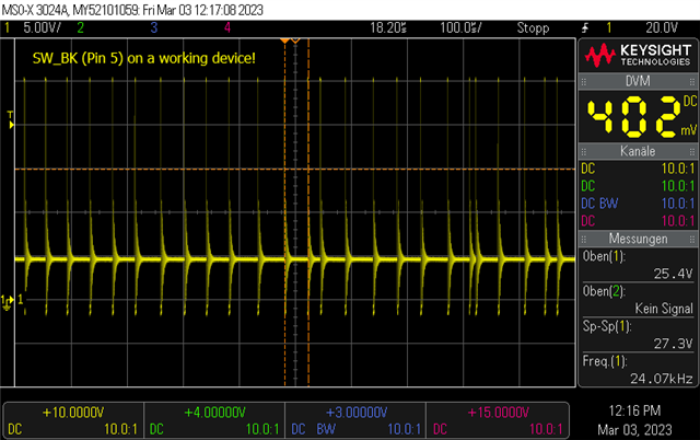
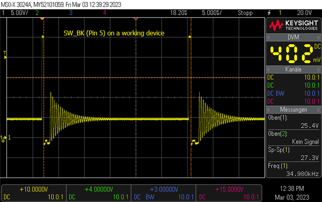
         Below is a screenshot of the PWM at SW_BK on a working device.

    The frequency on the SW_BK varies between ~10 and ~40 kHz. Is it normal?

    2) AVDD regulator input is VM or Buck output? (using the buck output generates less heat on the AVDD reg.)

    --> i don't see a  possibility to select between VM or Buck for AVDD Input. I think its always VM.

    Regards

    Michael M. 

  • Hi Michael,

    Could you please share the part number of the inductor on the buck output? We are worried that this inductor may be getting saturated at low currents.

    What are the external loads that VBK and AVDD is driving? MCT8316ZT has power sequencing enabled so VBK is also driving AVDD outputs.

    On a working board, how much current is being drawn by VBK?

    Could you power down the device and measure the resistance across VBK and PGND and SW_BK and PGND for a good unit and a bad unit?

    Monitor signal on SW_BK to check if the FET is switching on that node.

    Best,

    Robert

  • Hi Robert,

    we use the Würth 78438335470 inductor with the following parameters:

     We use the VBK for Hall supply only. Current concumption less than 10mA.

    On a bad device the resistance between VBK and GND is about 30 Ohm. It looks like it is nearly shorted to GND. 

    The mosfet is not switching.

    Best regards

    Michael

  • Hi Michael,

    Please allow me a couple days to look over the information you provided and respond by the end of the week.

    Best,

    Robert

  • Hi Michael,

    The inductor properties seem okay. 

    Somehow the VBK pin is experiencing leakage. The internal ESD cell may have been damaged and this can occur during overvoltage. 

    Can you please provide more details on any in-circuit tests or functional tests that could cause this damage?

    There are many ways to damage a pin so we just need all the exact details of the tests and environments that the ICs are being put under.

    Best,

    Robert

  •  Below is a screenshot of the PWM at SW_BK on a working device.

    Hi,

    The SW_BK has more than (negative) -5.1v during PWM off, which means the SW_BK pin driver is not running in synchronous upper and lower FET -- the lower FET should be ON to recirculate the inductive current. But the capture shows the oscillation voltage, so maybe the regulator mode was not selected correctly.

    i don't see a  possibility to select between VM or Buck for AVDD Input. I think its always VM.

    PS_PS_DIS selects which source for AVDD regulator.

  • Hello Brian, 

    we use the hardware variant of the IC. MCT8316ZT.

    I dont have the option to switch the BUCK_PS_DIS Bit. I guess VM ist the default Power supply for AVDD.

    Best Regards.

  • Hi Michael, Anthony,

    Any further assistance needed here?

    I am closing the thread for now since it was indicated above that this would be resolved over email.

    Please feel free to open a new question and link back to this one if there is additional support needs. Thanks! 

    Best Regards, 
    Andrew