This thread has been locked.

If you have a related question, please click the "Ask a related question" button in the top right corner. The newly created question will be automatically linked to this question.

DRV8323R: SPI communication error: wrong SDO data

Part Number: DRV8323R
Other Parts Discussed in Thread: DRV8323

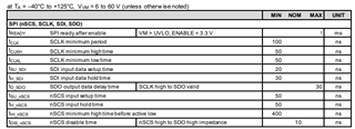
Clock frequency of sys_clk: 50 MHz;
Clock frequency of SPI_sck: 50 MHz/12.
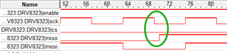
As shown in the figure, after CS is pulled low, I first configure the Gate Drive HS and Gate Drive LS registers:
Gate_Drive_HS = 16'b0_0011_011_1100_1000
Gate_Drive_LS = 16'b0_0100_111_1110_1110
Then read the values of Gate Drive HS and Gate Drive LS registers:
Gate_Drive_HS_RD = 16'b1_0011_000_0000_0000
Gate_Drive_LS_RD = 16'b1_0100_000_0000_0000
However, the SDO output signal of the DRV8323 chip is a bit delayed than my input signal, which causes the data I collect on the falling edge of SPI_SCK to be wrong.

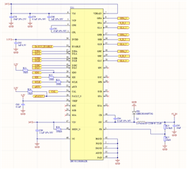
The peripheral circuit diagram of DRV8323RS is shown in the figure below.

  • Hi Wu,

    Thank you for posting this question! I will need to look into the information you sent and hope to provide further feedback by the end of the week.

    Best,

    Davis

  • Hi Wu,

    Please try sending a write command to unlock the registers via the LOCK field in the Gate Drive HS register (and not write anything else), and then send another write command with the actual data you want to write for both registers, and finally send one more write command to lock the registers (and not write anything else). Please let me know if this works.

    Best,

    Davis 

  • Dear Davis,

    I have identified the following parameters and sent them in order.

    IDRIVE_HS_Unlock = 16'b0_0011_011_0000_0000
    IDRIVE_HS              = 16'b0_0011_011_1111_1100
    IDRIVE_HS_Lock     = 16'b0_0011_110_0000_0000
    IDRIVE_HS_Read    = 16'b1_0011_000_0000_0000

    The signals sent and received by the FPGA are shown in the following picture.

    I first configured IDRIVE_HS, and when I locked IDRIVE_HS in the next step, the output signal of SDO was still wrong.

    Sorry I didn't see your reply until just now. Thank you for your help.

    Best Wishes,

    Wu

  • Hi Wu,

    Not sure if you're still having issues with writing to the register since you marked this thread resolved, but another combination to try might be to unlock the register, then lock the register but include the bits you want to write at the same time you are locking the register. If this doesn't work, please make sure there isn't a power cycle, sleep mode cycle, or UVLO fault before reading the register as these conditions cause the SPI registers to be set to default. Please let me know if either of these solutions help.

    Best,

    Davis

  • Dear Davis,

    Sorry I wrongly marked this thread resolved. I still have issues with writing to the register. I will try to unlock and lock the register including the bits I want to write and get back to you as soon as possible.

    Best Wishes,

    Wu

  • Dear Davis,

    IDRIVE_HS_Unlock = 16'b0_0011_011_0000_0000

    IDRIVE_HS              = 16'b0_0011_011_1111_1100

    IDRIVE_HS_Lock     = 16'b0_0011_110_1111_1100

    IDRIVE_HS_Read    = 16'b1_0011_000_0000_0000

    I've tried unlocking and locking the registers, including the bits I'm trying to write to. As you can see from the figure, the value I read after locking the register is the same as the value returned when I initially unlocked the register, but different from the value returned when I wrote to the register.

    I also tried to read 'Fault Status 1', as shown in the following figure, the return value is 0. The nFault pin is also not pulled low, indicating that the chip has not detected a fault.

    I am very confused why the chip's return signal jumps sometimes near the rising edge of SCK and sometimes near the falling edge of SCK. According to the manual, the chip should return data on the rising edge of SCK and receive data on the falling edge.

    Best Wishes,

    Wu

  • Hi Wu,

    I will need to do some more work to look into this issue and aim to provide more feedback by the end of the week.

    Best,

    Davis

  • I apologize for the delay, I will need to keep looking into this issue. Do you have an image of the MISO signal after the MOSI read signal has been sent? I am curious if the response is coming in the next frame of 16 clock cycles.

  • Hi Wu,

    Could you please clarify whether the delay in SDO is observed through a software producing the graphs above or through a real-time digital oscilloscope? From what I can tell in the graphs you have sent, the MISO signal looks correct after the read and register address command, with the small delay. This issue could be with the software view, rather than an delay in the output from the device.

    Best,

    Davis

  • Dear Davis,

    I captured MISO data using the 'Signal Tap Logic Analyzer' in the software 'Quartus'. This problem does not occur when I configure other chips, such as AD7386. I don't suppose that it's the software's problem.

    Best wishes,

    Wu

  • Hi Wu,

    Can you confirm if your SPI protocol is following these timing requirements?

    I am a little confused by the scale of the timing marker in the images you sent, and want to check in particular whether the SDO output data delay time might be causing the mismatch between the MISO signal and the clock. As far as I can tell, the returned read data on MISO appears shifted right by one bit in your images, but the bits themselves otherwise look correct.

    Best,

    Davis