This thread has been locked.

If you have a related question, please click the "Ask a related question" button in the top right corner. The newly created question will be automatically linked to this question.

MCT8329A: OCP_VDS & OCP_SNS Faults

Part Number: MCT8329A
Other Parts Discussed in Thread: MCF8329A

Hi All,

I have a custom board design that I have been working on and have run into OCP_VDS and OCP_SNS faults frequently. 

This issue seems to be random from board-to-board.  That is, of the prototypes I have tested, some immediately work, and some immediately fall into a fault condition.  Each board gets loaded with the same known 'good' registers before attempting to run. 

For the boards that fall victim to the fault, I have found that more often than not when a fault occurs the commutation FETs become damaged in high-side/low-side pairs, which led to the suspicion of cross-conduction.  I have been able to gather a lot of evidence to support this, and as a result have improved signal integrity and immunity, but have thus been unable to determine the root cause, and so, the problem persists. 

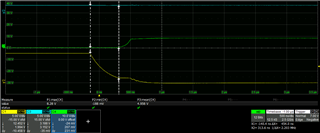
The following scope shots show the high-side and low-side gate drive signals during Startup alignment for a known good (able to run) board and a faulty board that immediately triggers an OCP_VDS fault:  Each board is identical in hardware and software.

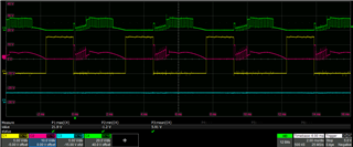
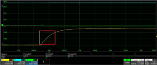
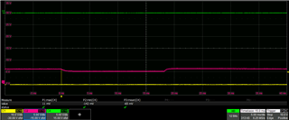
Good Board - Macro scale and zoomed in.  Red = high side;  Yellow = low side;  Green = CSA_OUT;  Input Voltage = 9V:

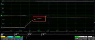
In this case, the board starts and runs at it should.  The high-side gate is being pulled Low as the low-side gate is pulled High.  Even though the board runs, I still suspect some amount of cross-conduction as both gate voltages converge slightly above the gate threshold voltage.  If I increase the input voltage to >22V, a OCP_SNS condition is to be expected as each gate voltage will be slightly higher.  If, in this case, cross-conduction is occurring, then it is not enough to trigger a fault condition, and may or may not be true up to ~22V.

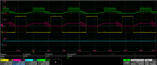
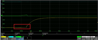
Faulty Board - Macro scale and zoomed in.  Red = high side;  Yellow = low side;  Green = CSA_OUT;  Input Voltage = 9V:

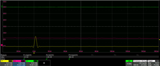
The above scope shots were taken during startup on one of the faulty boards.  As we can see, as the low-side gate gets pulled high during initial alignment, the high-side gate fails to get pulled low.  In this condition, it is suspected that both high-side and low-side FETs are effectively conducting leading to a cross-conduction condition. This would explain the OCP_VDS fault trigger.  I also suspect that if I increase the input voltage that I will trigger either an OCP_VDS fault or an OCP_SNS fault and likely damage the FETs - this has been the case on other boards.  The reason to start with a low (9V) input voltage was to hopefully prevent damage to the FETs while attempting to solve the issue (thus far, it does not seem as if my FETs have been damaged, but the fault persists).

My investigation into this issue has been extensive both in terms of hardware and in software.  I have tested for undesired shorts and opens, and compared the measured point-to-point impedances and component values of the 'good' board to the 'faulty' board used in this data collection and have only found negligible variations due to tolerances.

I am here now in hopes that someone may be able to offer some insight into:

  • What might be the cause of the High-side gate not being pulled low during startup
  • What I might be able to check for (chances are good that I have already)
  • The likeliness that this is a design/layout issue, and why it would be so random/unpredictable from board-to-board
  • The likeliness that this an IC (MCT8329A) issue
  • If it is common, and if there is a known fix

I understand you may not be able to answer all my questions, but I am running out of directions whilst chasing this problem.  Any and all insight will be greatly appreciated.

Thank you for your considerations.

  • Hello Ben,

    Can you provide me a capture of GHx, GLx, SHx, and VM voltages? If possible please use a tip-in-barrel probe to measure the GHx and GLx signals.

    What I might be able to check for (chances are good that I have already)

    If you preform a ABA test, swapping a good device on a good board with a bad device on a bad board, does the issue follow the board or the device?

    If you have not already, can you increase the DIG_DEAD_TIME to 500ns or greater and see if this improves the performance?

    If it is common, and if there is a known fix

    We have a FAQ for debugging Common issues in BLDC motor drivers which may provide some more debug tips.

    Regards,

    Joshua

  • Hi Joshua,

    Thank you for the reply. 

    Can you provide me a capture of GHx, GLx, SHx, and VM voltages? If possible please use a tip-in-barrel probe to measure the GHx and GLx signals.

    I have not attempted the tip-in-barrel method, but I was able to get one of my problem controllers running.  The original scope shots that I shared were from a different board that I believe may be an isolated issue since the gate drive signals are not being pulled low as they should.  I am yet to see this on another board.

    I'd like to share with you a few scope shots taken from a board that initially failed at startup.  An SNS_OCP fault was triggered and one of the high side FETs was shorted, I replaced it, but it would immediately trigger a VDS_OCP fault.  I was able to get it to run by disabling the VDS_OCP fault, though poorly, and we can see why by the scope. 

    These shots were taken close to the gate drive pins on the IC (before the GDR).

    Yellow:  Low side Gate;  Green:  High side Gate;  Red: Phase [A] output

    Yellow:  Low side Gate;  Green:  High side Gate;  Red: Phase [B] output

    Yellow:  Low side Gate;  Green:  High side Gate;  Red: Phase [B] output

    **For this shot it appears I forgot to move the probe from Phase B to phase C, but it offers insight into how the low side switching of phase C is affecting the phase output on Phase B...

    These shots were taken under "no load" conditions - only static mechanical losses.  To me, there are a number of different things to observe here, but the most concerning is the high duty cycle under the no load conditions.  It also appears that the FETs are not properly turning off based on the PWM switching, but it is difficult to determine if the problem is with the FETs or if it is with the gate drive signals.

    If you preform a ABA test, swapping a good device on a good board with a bad device on a bad board, does the issue follow the board or the device?

    The problem seems to follows the boards, not the device.  I have a handful of 'good' boards that I can swap out interchangeably between various devices with various tuning parameters and they have no problem driving the motor as expected.  As I said before, the problem seems to 'random' from board to board, making it unpredictable whether a previous unused board will work properly or not.

    If you have not already, can you increase the DIG_DEAD_TIME to 500ns or greater and see if this improves the performance?

    This does not help.  I have also tried adjusting the de-glitch and blank out times but nothings has helped.

    We have a FAQ for debugging Common issues in BLDC motor drivers which may provide some more debug tips.

    I started poking through this yesterday and will have another look to see if there is something I missed.

    BenG

  • Hi Mikael,

    Could you provide me the schematic for the MCF8329A including the external half bridges?

    During the ABA test did you take MCT8329A from a bad boards and move them to a good boards and was the MCT8329 able to drive a motor without any issue? I would like to confirm that the MCT8329A on the bad boards are not being damaged.

    Regards,

    Joshua

  • Joshua,

    Could you provide me the schematic for the MCF8329A including the external half bridges?

    I would be happy to, but I would rather not do so publicly.  Would we be able to discuss details of the schematic privately?

    During the ABA test did you take MCT8329A from a bad boards and move them to a good boards and was the MCT8329 able to drive a motor without any issue? I would like to confirm that the MCT8329A on the bad boards are not being damaged.

    Forgive me, I must've misunderstood the ABA test.  I did not swap ICs but instead the entire board.  I will attempt this today, but - from experience - will be a difficult and delicate task.  It may be worth it, however, as I've had the idea in my head that it could be a layout problem and the minor variances from board to board may be enough to trigger the issue.

  • Hi Ben,

    I sent you a friend request so that we can discuss the schematic in a private chat.

    Regards,

    Joshua

  • Joshua,

    I wanted to measure and observe the effects of the DIG_DEAD_TIME at various intervals; 50ns, 500ns, and 1000ns.  The following scope shots were taken from a new board - that is, factory sealed before attempting to run.  I loaded known good register settings and the board had no issues starting up; it seems to run well at [least at] low voltages (<9V input).  It has been found that many of the OCP issues I have been facing are associated with higher input voltages, presumably because this raises the gate drive voltages as well.  I have not tried starting the motor at a higher voltage, yet, but I did inch the voltage up to 20V while it was running to make sure it didn't fault.  It did fine, but my application still requires me to be above that. 

    Screen shots of Gate Drive Signals:  Yellow = Low-Side, Red = High-Side, Blue = nFault (never triggered). 

    Note:  For the last three images, I circled a unique transient that was observed when changing the dead time.  This was repeatable, and it's position in time is dependent on the DIG_DEAD_TIME setting.  Unfortunately, I lack a good understanding of this.

    •   DIG_DEAD_TIME = 50ns; Low-Side [OFF];  High-Side [ON];

    •   DIG_DEAD_TIME = 500ns; Low-Side [OFF];  High-Side [ON];

    •   DIG_DEAD_TIME = 1000ns; Low-Side [OFF];  High-Side [ON];

    •  DIG_DEAD_TIME = 50ns; Low-Side [ON];  High-Side [OFF];

    •  DIG_DEAD_TIME = 500ns; Low-Side [ON];  High-Side [OFF];
    •  

    • DIG_DEAD_TIME = 1000ns; Low-Side [ON];  High-Side [OFF];

    Conclusion:  Changing the dead time duration does not seem to cause a measurable change in the length of time between the High and Low side switching of the gates.  If not for the unique transient that was observed, there would have been no other indicator that the dead time was being introduced at all.  From the datasheet:

    "7.3.2.1 Dead time and Cross Conduction Prevention
    The MCT8329A provide digital dead time insertion between the high side and low side PWM signals, to prevent
    both external MOSFETs of each half-bridge from switching on at the same time. Digital dead time can be
    adjusted between 50 ns and 1000 ns by configuring EEPROM register DIG_DEAD_TIME."

    With all this being said, I am of the opinion that one or more of the following things is true:

    • I am missing something in hardware
    • I am missing something in software
    • I do fully understand how Digital Dead Time works
    • The IC is failing to properly insert dead time

    Hopefully you can provide some illumination into the matter,

    Thank you

  • Hello Ben,

    Please allow me some time to look at the information you have provided. I will aim to get back with you by next Thursday.

    Regards,

    Joshua