


Debug of issues vary from situation to situation, but over time you will start to recognize patterns between the common problems. The following are some of the most frequently asked questions and methods for solving them. Always remember debugs come down to the inputs and the outputs, so the key to figuring out the issue lies in tracing back where the problem is originating from.
Please monitor the driver for any faults being triggered and use them as a guide while consulting the suggested debugs below.
List of commonly faced issues:
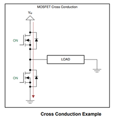
1. MOSFET Shoot-through aka Cross-Conduction
Description:
- During normal motor commutation, phase current will conduct through either low-side (LS) or high-side (HS) MOSFET in a half-bridge configuration. If both HS and LS are conducting partially or fully at the same time, then a shoot-through condition occurs and creates a low-resistance high-current path between high-voltage and ground. This can potentially damage the PCB system and its components including the MOSFETS.
- Many DRV devices typically include a feature called automatic ‘dead-time insertion’ which can prevent the shoot-through condition described above.
Verify:
- Waveforms:
- Check if GHx and GLx are conducting at the same time.
- Check the VDS waveform to confirm rise/fall times.
- Check INHx and INLx of the same phase to see if inputs are being sent at the same time (might be okay if deadtime can compensate).
- Damage:
- Check if there is a short between drain to source of the MOSFETS.
- Check to see if there is a visible burn on the gate driver outputs or the MOSFETS.
Debug:
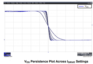
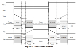
- Gate Current: Check to see if the IDRIVE setting being used is too high. IDRIVE determines how fast the gates slew on/off (consult figure below). You can lower the IDRIVE or add gate resistors to reduce gate current and increase the rise/fall times. We typically recommend a rise/fall time of 100-200ns for fast switching and to avoid most ringing/EMI.
Trise/fall = QGD / ISource/Sink
- Deadtime: Depending on the commutation mode there will be automatic deadtime (time between one MOSFET turning off and the other turning on) inserted to prevent cross conduction. However, we suggest users to increase deadtime to reduce chances of both MOSFETS switching at the same time.
- Increasing the rise/fall time too much can increase the thermal loses in your MOSFETs while decreasing your rise/fall time too much can increase chances of shoot-through or EMI problems. It is important to find a balance between too fast and too slow depending on your application and system needs.
- MOSFET QGD: If the MOSFET QGD is too small then it might lead to fast rise/fall times based on the equation above.
- Resources:
- Examples:
2. GVDD dips
Description:
- There is a dip in GVDD when starting the motor. This is expected as when the motor is starting the GVDD is being used to charge the bootstrap capacitors while the low side is on. So, we see a small ripple on GVDD.
- This is an issue if the GVDD stays lows for a long period of time and might point to other issues covered below.
Verify:
- Waveforms:
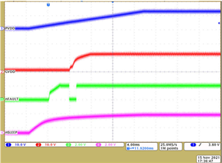
- Measure GVDD at the motor startup to see if there is a dip (how low?) and to see if the GVDD voltage comes back to nominal voltage or if it stays low.
- Waveform showing GVDD during powerup
Debug:
- GVDD capacitor: If the GVDD cap is placed far from the device, then it can lead to inductance being added through the length of the trace. Another reason might be that the GVDD cap value is too low, which prevents it from being an effective bulk capacitor at regulating the voltage at GVDD.
- IDRIVE: Suggest lowering IDRIVE. Some devices have the highest IDRIVE setting as default.
- Examples:
3. Excessive Heating
Description:
- Some customers report seeing high junction temperatures on the IC leading to concern.
- Sometimes the MOSFET might be over heating while other times it might be the driver or both depending on the specific use case.
- Thermals are a big concern with integrated FET drives since there is less area for thermal dissipation.
Verify:
- Temperature collection: Collect temperature of the IC using an infrared camera to see if there is excessive heating and compare this to the absolute maximum junction temperature listed in the datasheet to see if there is a spec violation.
- Physical damage:
- Check for physical burn or shorts on the driver IC. Typically seen near motor outputs pins, VCP, or near VM.
- Check for short on the MOSFETS in event of a shoot-through.
Debug:
- IDRIVE: Suggest lowering IDRIVE. Check if they follow the correct rise/fall time recommendations.
- Motor Specifications: Inquire about their motor current draw to see if that maybe the reason for heating.
- Deadtime: suggest increasing deadtime to reduce the time the MOSFETs conduct
- PWM: Please follow the recommended PWM frequency range in the datasheet. Higher frequency can result in increase in switching losses and lead to heating.
- Layout:
- Poor layout can lead to bad thermals.
- Check to see if appropriate trace width is being used (1A~10mil)
- Check for proper grounding.
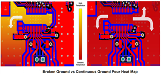
- Consider doing a layout review and a comparison with our EVMs.
- Resources:
4. Mosfet not switching
Description:
- During testing you might get an issue of the MOSFET outputs not matching the expected outputs. This can include instances when the motor stops spinning, never spins, or spins in an erratic manner. These issues can stem from error in commutating the motor, damage to the MOSFETs, issues in setting the correct PWM signal etc.
Verify:
- Waveforms:
- First step would be to identify the motor outputs. So, begin by collecting waveforms of GHx and SHx.
- Collect waveforms of the INHX and INLX signals to see if the input signals are being provided correctly.
Debug:
- Check for correct gate turn on behavior and ensure there is no MOSFET shoot through condition. It is recommended to start with low IDRIVE settings.
- Deadtime: Identify if the deadtime being set by the user is being translated to the outputs. Refer to the following diagram for help.
- PWM signal: Identify the user’s desired PWM mode and check if the GHx signals match truth table in the datasheet. If there is error in setting the PWM signals, check via a SPI read out or by checking the schematic and the voltages being set for the hardware devices.
5. Unused phases, spinning brushed motors
Description:
Sometimes users would like to use our drivers for spinning brushed motors. This would require the use of only two of the three phases. Therefore, one would need to address the inputs and the outputs of the unused phase.
Debug:
- Varies slightly from device to device on what all pins are involved.
- INHx/INLx = connect to GND (non-inverting)
- INHx = connect to GND and INLx = connect to 3.3V (inverting, DRV8300)
- BSTx = floating
- GHX/GLX = floating
- SHX = connect to GND
- Do populate GVDD to BSTx diode when applicable even for unused phases
- Resources:
6. Unused CSA
Description:
- When the internal CSA is not being used, the goal is to prevent the toggling at the CSA outputs.
Debug:
- CSA inputs, SPx and SNx = tied together and connected to GND
- CSA output, SOx = floating
- Resources:
7. Schematic Review
Description:
- An evaluiation of the schematic for proper part selection and wiring before producing a layout and PCBs.
Debug:
- Datasheet: Check values of external components and placements based on Pin Functions table and External Components table. Ensure correct value and voltage rating.
- EVM: Compare the design implementation based on our EVM’s schematic.
- Additional components: Sometimes users might benefit from the addition of external components to better improve the performance of their system or to reduce chances of failure. So please consult the design resources below.
- Resources:
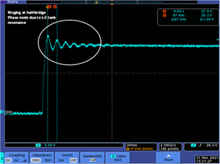
8. Ringing at outputs
Description:
- When switching high currents at the MOSFETS, some users might observe ringing at SHx. These can result from parasitic inductance or capacitance and from a less than ideal PCB design.
- The ringing can lead to EMI concerns, poor device performance and issues in high power dissipation.
Verify:
- Waveforms:
- Check the waveforms of phase outputs, SHx, to see if there is ringing present as seen in the waveform below.
Debug:
- Implement an RC snubber to reduce the oscillations
- Lower IDRIVE setting
- Add additional gate resistance
- Resources:
9. High side or Low side pre-driver undervoltage (VCPUV, VGLS dip, GDUV)
Description:
- Issues in driver outputs can stem from errors in the pre-drivers.
- When you notice users having GDUV it is possible that the error stems from faults in VGLS or VCP operation. Sometimes VCP/VGLS might be below the needed threshold or might experience frequent dips
Verify:
- Waveforms: Collect VM, GHx, VCP and VGLS waveforms and check to see if any undervoltage or “dips” occur.
Debug:
- Check to see if there is a drop in VM corresponding to the undervoltage being observed.
- Check to see if the charge pump capacitors (VCP-Vdrain, CPH-CPL) are placed close to the driver in the layout. Check is VGLS cap is placed close to VGLS pin in layout.
- IDRIVE: Check MOSFET QGD and IDRIVE to ensure appropriate rise/fall times. This can cause ringing at the gates/sources during switching. This might result in voltage rating violations which can lead to damage.
- SPI: Check if SPI is getting reinitialized to use the highest IDRIVE setting when VM<UVLO or when enable =LOW (sleep mode)
- Resources:
10. Recommended Operating Condition vs Absolute Maximum
Description:
- Recommended operating conditions refer to the range in which we expect our drivers to provide the output specified in the datasheet. We recommend operating devices at the typical/nominal value for optimal performance and reliability.
- Absolute maximum is the maximum rated value a specific pin can handle. This does not mean that the device will work as intended if used at this stage. This can also lead to damage and can significantly affect device lifetime and reliability.
- If used outside the Recommended Operating Conditions but within the Absolute Maximum Ratings, the device may not be fully functional, and this may affect device reliability, functionality, performance, and shorten the device lifetime.
Debug:
- Confirm the operating conditions and check if the operation is within specified limits.
- Check if the conditions described are nominal operating conditions or just transients. Datasheets typically mention if pins can handle transients (amount + duration)
- Resources:
11. Layout Review
Description:
- Layout reviews are critical in ensuring proper device operation.
- Can be used to identify any issues seen in outputs and serves as a useful tool for debug.
- Main considerations involve placement of components, trace widths, and parasitics.
Debug:
- DRV-related: place bulk and bypass capacitors as close as possible to the DRV device (VCP, CPH-CPL, VM, VGLS, DVDD, AVDD, PVDD, GVDD, etc.). DRV caps should be placed on the same layer of the PCB as the DRV to ensure that there is not added inductance due to vias placed in the capacitor path.
- Gate drive-related: gate drive outputs routed as short and wide as possible, with a recommended width of at least 15-20mil to mitigate parasitic effects
- Power stage-related: motor current paths routed using copper pours, repeated layers, and thermal/stitching vias to minimize parasitics
- Supply/GND related: proper placement and layout of supply paths, bulk capacitances, and sufficient grounding strategies to provide current return paths
- Analog related: fast switching signals routed differentially with filtering components placed near input pins of IC
- Digital related: fast switching signals routed differentially with higher priority over slow switching signals
- Resources:
Additional Resources:
