This thread has been locked.

If you have a related question, please click the "Ask a related question" button in the top right corner. The newly created question will be automatically linked to this question.

DRV8329: CSAGAIN Setting

Part Number: DRV8329

hello, 

I am using DRV8329 to spin 3 Ph BLDC motor on one of our Project. this is a key project we are working and has very high annual volume ( > 50k)

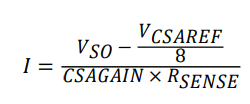
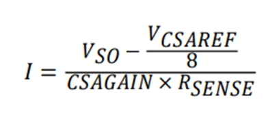
we are evaluating the possibility of using CSAGAIN and SO pin to read the current from Motor and have Connected CSAGAIN To GND to read max current. Peak current (motor phase) in my application could go up to 90A during startup at load. 

I am getting good data on the SO Pin but the voltage does not match with gain mentioned in the datasheet. 


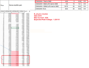
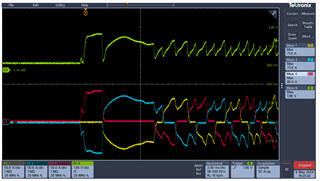
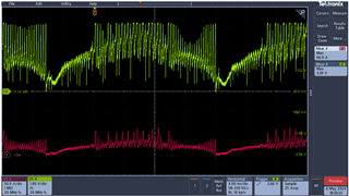
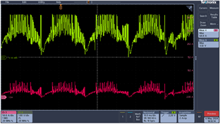
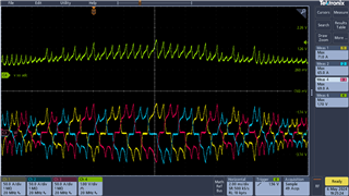
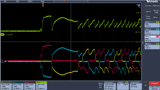
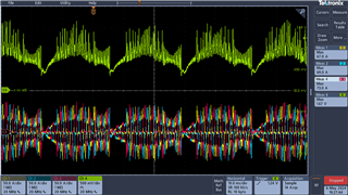
with CSAGAIN to GND I calculated table in above image. below are scope captures of Motor Phase current peak value and SO pin voltage wrt GND. there is clear offset of 400mV to 800mv which is very high. see below captures for reference 

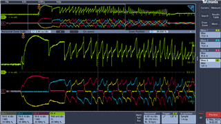
Peak current at startup is 81A, according to table, SO Voltage should be close to 1.24V but i am seeing 1.92V here, some more images below during operation 

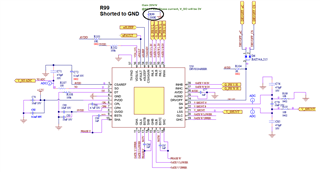
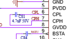
Request you to provide some feedback on the discrepancy observed. Below is snapshot of DRV8329 section. 

  • Hi Abishek

    with CSAGAIN to GND I calculated table in above image.

    What formula are you using for this calculation? 

    When did this issue start? Was there a point where the device behaved properly at peak current?

    Regards,

    Yara

  • Hello, 

    this is a formula from datasheet. 

    we initially were focused on other functionalities of tool and when we started validating overload protection, we looked at SO voltage measurement. therefore the readings are same, so i believe issue is from beginning.

    CSAREF is pulled to AVDD as you can see in the snap. 

    Regards

    Abhishek  

  • Another Question on different topic though, 

    How DRV8329 will recover from DRVOFF Fault.? means when DRVOFF is pulled to AVDD, Output Gates are Turned OFF irrespective of input at Gate Driver. so in this case there will Gate pulses present at input but o/p will be floating. with this situation, motor will stop due to no active driving. Current will drop to lower value and if DRVOFF is pulled down, Motor will start spinning again immediately ? No need to clear any Fault. Is my understanding correct ? 

  • Hi Abhishek,

    I think the "offset" you are seeing is really just Vcsaref/8. You would need a negative current to actually get Vso to equal 0 because if you have 0 current then Vso would equal equal 400mV. Is this what you are seeing across all gain setting or only 5V/V?

    and to answer your second question

    Regards,

    Yara

  • Hello Yara, 

    you are correct, i do see offset of ~400mV. it can be seen in the waveforms as well which are attached in 1st post. even if i subtract that offset, peak value of current and peak value of  SO voltage does not match. This is main issue. Offset is going up to 800mV in some cases or even more. 

    For peak current of 85A, with offset of ~420mV, peak value is 1.98V and with Calculation by formula, it should be ~1.27V. 

    it becomes difficult  to put formula in firmware to get close to accurate current reading. 

  • Hi Abhishek,

    Is this offset consistent across all the gain settings? Meaning is the offset greater when using 20V/V for the gain setting?

    Regards,

    Yara

  • Hi Yara, yes higher offset is at 10V/V as well. i had connected 50k. you can see waveform below. 

    SO voltage is saturating to 3.3V at 65A only. if you refer the graph above again 

    with 10V/V, at 65A, the max value should be close to 1.68V but SO voltage is already saturated.

    so it seems the offset ERROR is amplifying with higher gain


  • Hi Abhishek,

    I'll need a couple of days to look into this more thoroughly. I'll have an update by the end of the week.

    Regards,

    Yara

  • Hi Yara, 

    has there been any update. we would like to close the issue now and understand if we can reduce the offset or not. This decision will help us to make use of uC ADC pin for some other application and go ahead with conventional Op amp based current measurement. 

  • Hi Abishek,

    Apologies for the delay. I took a closer look at your schematic and it seems like the value for the charge pump capacitor is incorrect

    it should be 470nF or 0.47uF

    This is a critical component and should be changed, and hopefully this will resolve your issue.

    I also made a table based on the min and max value for CSAREF and CSA GAIN variable in this equation

    VSO Calculations.xlsx

    Let me know if your issue is resolved

    Regards,

    Yara