This thread has been locked.

If you have a related question, please click the "Ask a related question" button in the top right corner. The newly created question will be automatically linked to this question.

DRV2700: Output protection

Part Number: DRV2700


Tool/software:

Hi TI Team,

We are currently working with the DRV2700 in our design and have encountered an issue during FEMA testing.

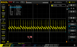
Under the conditions where the EN pin is enabled and a signal is provided to IN+, we intentionally shorted OUT+ to OUT– (and also tested with OUT+ shorted to GND). During this short circuit, the total system power consumption spiked to approximately 5 W (for reference, the standby power consumption with EN enabled is about 0.7 W).

After maintaining the short circuit for a few seconds and then removing it, we observed that the system power consumption did not return to normal levels—even after re-powering up the device. Additionally, we noticed that the input inductor (XFL4020-472MEB) reached temperatures exceeding 100°C. Upon removing and testing the inductor, we found its inductance had degraded to about 2 μH. After replacing the damaged inductor with a new one, simply enabling the chip (without any load) resulted in a power consumption of 2 W and the chip heating up to around 60°C. This suggests that both the DRV2700 and the inductor were damaged due to the short circuit on the output.

Our circuit configuration is as follows:

  • REXT: 10 kΩ
  • Rfb1: 806 kΩ
  • Rfb2: 10.5 kΩ

We have a few questions regarding this issue:

  1. Inductor Damage: Based on the power consumption during the short circuit, it seems the input current did not reach the inductor's saturation current nor the current limit set by REXT. Why did the inductor fail under these conditions?

  2. Protection Mechanisms: Does the DRV2700's thermal shutdown feature not activate in this scenario? Are there any overcurrent protection mechanisms inherent to the chip that should prevent this kind of damage?

  3. Output Signal Considerations: Our application requires a DC step output, potentially transitioning from 0 V to 100 V instantly. If overcurrent is a concern with such rapid voltage changes, would you recommend implementing a slew rate limitation to mitigate this issue?

Thank you for your assistance!

Kind regards,

Cain

  • Hi Cain,

    The devices thermal protection only kicks in when the device itself reaches an above threshold temperature. There is not any short circuit protection on this device. There was likely a large current spike at the beginning that damaged the device and the inductor. There is no problem to go from 100V and then disable (EN low) the device to get 0V. The issue will arise if you short the outputs. 

    Regards,
    Sydney Northcutt 

  • Hi Sydney,

    Thank you for your prompt response.

    I have a follow-up question regarding the voltage transition from 0 V to 100 V.

    In our normal operation, we use a square wave (IN+) below 1 Hz to drive a load of approximately 6 μF. It appears that, albeit with very low probability, similar overcurrent issues can be triggered during these transitions—specifically, the inductor overheating and potential chip damage. Could this also be caused by current spikes when rapidly charging the capacitive load from 0 V to 100 V?

    Does TI recommend adding a series resistor at the output to limit the inrush current in such cases? If so, is there a recommended resistor value or any guidelines on how to select an appropriate value to mitigate this issue without adversely affecting the performance?

    We appreciate your assistance and any insights you can provide to help us resolve this problem.

    Kind regards,

    Cain

  • Hi Cain,

    I will provide a response tomorrow. Thank you for your patience!

    Regards,
    Sydney Northcutt

  • Hi Cain, 

    My apologies for the delay here! I don't expect this behavior with your load.. It would likely drain the boost current causing the boost voltage to drop but I believe the boost should recover. 

    Could you provide schematic and layout documents? If you prefer to share this over email let me know and I can start a thread. 

    Regards,
    Sydney Northcutt 

  • Hi Sydney,

    Thank you for your response.

    Could you please initiate an email thread so we can send you our schematic and layout?

    In the meantime, I have a few follow-up questions:

    1. Series Resistor at the Output:

      • We were wondering if adding a series resistor at the output would be recommended to limit inrush current when driving large capacitive loads (we're using around 6 μF). Would you advise this approach? If so, how should we select an appropriate resistor value?
    2. Boost Voltage Drop:

      • We've observed that when applying a step input to IN+, the boost voltage drops from 100 V down to around 20 V. Is this expected and safe behavior during such transitions?
      • Additionally, when IN+ is left floating, it appears to be at around 2 V. If we want to add a pull-down resistor to prevent noise when IN+ is floating, what resistor value would you recommend?
    3. Feedback Voltage :

      • The feedback voltage we're measuring is about 1.4 V instead of the expected 1.3 V per the datasheet and simulations. During inductor operation, there are also spikes on the feedback line, peaking up to 1.6 V.
      • Could these higher feedback voltages and spikes potentially lead to chip failure?
      • Our Rfb resistor values are set for a theoretical boost voltage of 101 V, but we measure around 104 V. We've noticed that setting the boost voltage slightly above 105 V can lead to some chips failing after a period of operation. Could the elevated feedback voltage and spikes be contributing to this issue?
      • Waveform of feedback voltage using x10 probe: 

    Best regards,

    Cain

  • Hi Cain, 

    Sure please expect an email shortly.

    Can you explain what you mean by chip failure here? If you mean the boost voltage dropping, it should recover and there should not be damage to the device. With the 6uF load, are you seeing the device or boost inductor having some damage and no longer being functional? The issue is not how quickly the current is going to the load, it's how much current the load is pulling. The boost is only capable of about 1mA at 100v. The case could be that this capacitor is just too large for the device to handle. Is it possible to use some lower capacitance load?

    The different FB voltage should not cause any damage and it is expected to vary slightly. Let me do some testing on my end to ensure its within the expected range, but I don't believe this is the issue here. 

    If you are wanting to do single ended input, you could tie in- to ground with a capacitor. 

    Regards,
    Sydney Northcutt 

  • Hi Sydney,

    I've sent our schematic and layout via email as you suggested.

    Regarding the "chip failure" I mentioned, the specific issues we're encountering are detailed in the email attachments.

    And yes, we are concerned that with our current load capacitances, the current drawn may exceed the chip's capabilities. We have two types of loads, specifically 3.4 μF and 6.8 μF, and we've experienced failures with both. Our input step signal has a rise time of about 4 μs. Even though the operating frequency is low, should we consider limiting the rise time according to Figure 8-2 in the datasheet to avoid overloading the chip? We've noticed that when IN+ is left floating or when driving with higher frequency square waves, the instantaneous power consumption can occasionally exceed 1 W.

    Regarding the feedback signal, as described in the email attachments, in earlier versions we encountered signal interference that caused the boost voltage to exceed 105 V, resulting in simlilar chip damage. We've since optimized the layout and reduced the preset maximum voltage to 101 V. However, based on the current feedback waveform, we're unsure if the safety margin is sufficient.

    Kind regards,

    Cain

  • Hi Cain, 

    Understood. I will follow up on our email thread.

    Regards,
    Sydney Northcutt