This thread has been locked.

If you have a related question, please click the "Ask a related question" button in the top right corner. The newly created question will be automatically linked to this question.

DRV8305: SPI write/read issue ?

Part Number: DRV8305
Other Parts Discussed in Thread: LAUNCHXL-F28379D, , LAUNCHXL-F28027F, , MOTORWARE, CONTROLSUITE

Tool/software:

 Hi Team,

I am using DRV8305 booster pack with LAUNCHXL-F28379D board.

I have configured SPI A to communicate with the the booster pack via SPI.

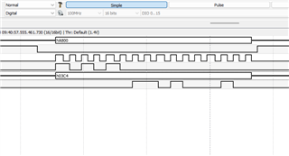
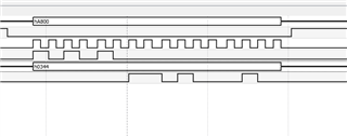
I am trying to write and read back the SPI registers to confirm whether SPI is working or not.

I observe that SPI write is not happening successfully. I am reading back the register after writing to it.

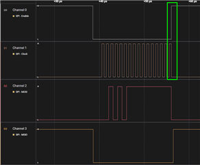
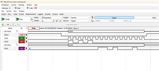
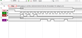
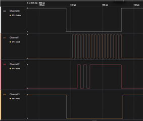
Bellow is the waveform of write command - 0x2BFF; /*0b00101 011 11111111*/;     

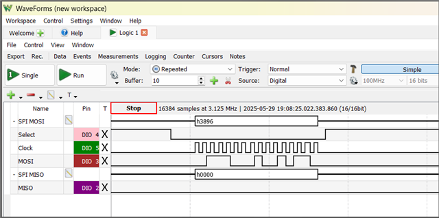
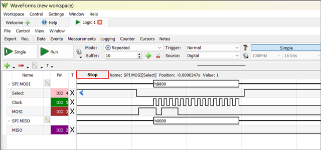
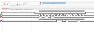
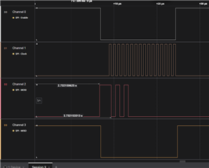
And below is the waveform of read command - 0xA800; /*0b10101 000 00000000*/;

_

I have provided 20 volts to the Booster pack and also set the EN_GATE pin

This is how my code looks like:

    while(1)
    {


        SPI_writeDataNonBlocking(SPIA,0x2BFF);
        r1Data = SPI_readDataBlockingNonFIFO(SPIA);
       
        DEVICE_DELAY_US(10000);
       

        SPI_writeDataNonBlocking(SPIA,0xA800);
        r1Data = SPI_readDataBlockingNonFIFO(SPIA);
}
  • Hi Team, we need an update on this.

    Can you please provide us with an update ?

  • Team, please assist on this 

  • Hi Sourabh,

    Can you confirm that nSCS is held down long enough so that it is low at least 50ns after the last clock pulse?

    another request, can you read all the registers and ensure that you are reading back the default values?

    Regards,

    Yara

  • Hello Team,
    Below is the code in which we added delay after last clock pulse goes low and CS goes high.
    We have programmed GPIO61 to be used as CS.
    Also we have enabled WAKE and EN_GATE pins of DRV8305EVM with around 30ms delay which is greater than the recommended 10ms time tSPI_READY (SPI read after power on). 

    #include "driverlib.h"
    #include "device.h"
    
    void initSPIA(void);
    void initGPIOForSPIA(void);
    //interrupt void spi_isr(void);
    void main(void)
    {
        // Initialize device and disable interrupts
        Device_init();
    
        //
        // Disable pin locks and enable internal pullups.
        //
        Device_initGPIO();
    
        //
        // Initialize PIE and clear PIE registers. Disables CPU interrupts.
        //
        Interrupt_initModule();
    
        //
        // Initialize the PIE vector table with pointers to the shell Interrupt
        // Service Routines (ISR).
        //
        Interrupt_initVectorTable();
    
        //
        // Interrupts that are used in this example are re-mapped to ISR functions
        //
        //Interrupt_register(INT_SPIA_RX, &spi_isr); // read SPI interrupts first and then reconfigure if required 
    
        // Initialize GPIO for SPIA
        initGPIOForSPIA(); 
    
    
        // Initialize SPIA as master
        initSPIA();
    
        // Enable global interrupts
        EINT;
        ERTM;
    
        uint16_t txData = 0x3896;
        volatile uint16_t rxData;
        volatile uint16_t rxData1;
        volatile uint16_t rxData2;
    
        while(1)
        {
        
            //CS_low();
            GPIO_writePin( 61, 0);
            // Send data
            SPI_writeDataBlockingNonFIFO(SPIA_BASE, txData);
            // Read received data
            rxData = SPI_readDataBlockingNonFIFO(SPIA_BASE);
            DEVICE_DELAY_US(1); // 1 us delay before chip select goes high
            //CS_high();
            GPIO_writePin( 61, 1);
            // Optional: insert delay if needed
            DEVICE_DELAY_US(1000);


            //CS_low();
            GPIO_writePin( 61, 0);
            // Send data
            SPI_writeDataBlockingNonFIFO(SPIA_BASE, 0xB800);
            // Read received data
            rxData1 = SPI_readDataBlockingNonFIFO(SPIA_BASE); 
            DEVICE_DELAY_US(1); // 1 us delay before chip select goes high
            //CS_high();
            GPIO_writePin( 61, 1);
            // Optional: insert delay if needed
            DEVICE_DELAY_US(1000);
    
    
        }
    }


    void initSPIA(void)
    {
        //***********************
        // Reset the SPI module
        SPI_disableModule(SPIA_BASE);
        //SPI_resetModule(SPIA_BASE);
    
        // Set the SPI configuration
        SPI_setConfig(SPIA_BASE, DEVICE_LSPCLK_FREQ,
                      SPI_PROT_POL0PHA1,      // Polarity 0, Phase 1
                      SPI_MODE_MASTER,        // Master mode
                      1000000,                // Baud rate = 1 MHz
                      16);                    // 16-bit word size
    
        // Enable FIFO (optional)
        SPI_disableFIFO(SPIA_BASE);
        SPI_clearInterruptStatus(SPIA_BASE, SPI_INT_RXFF);
    
        // SPI_enableInterrupt(SPIA_BASE,SPI_INT_RX_OVERRUN);
        // SPI_enableInterrupt(SPIA_BASE,SPI_INT_RX_DATA_TX_EMPTY);
    
        // Enable SPI module
        SPI_enableModule(SPIA_BASE);
        //***********************
       
    
    }
    
    
    void initGPIOForSPIA(void)
    {
        EALLOW;
        // Configure GPIO58 as SPIA SIMO (Master Out, Slave In)
        GPIO_setPinConfig(GPIO_58_SPISIMOA); // for master out slave in (MOSI) functionality
        GPIO_setDirectionMode(58, GPIO_DIR_MODE_OUT);
        GPIO_setPadConfig(58, GPIO_PIN_TYPE_STD);
        GPIO_setMasterCore(58,GPIO_CORE_CPU1);


        // Configure GPIO59 as SPIA SOMI (Master In, Slave Out)
        GPIO_setPinConfig(GPIO_59_SPISOMIA); // for master in slave out (MISO) functionality
        GPIO_setDirectionMode(59, GPIO_DIR_MODE_IN);
        GPIO_setPadConfig(59, GPIO_PIN_TYPE_STD);
        GPIO_setMasterCore(59,GPIO_CORE_CPU1);
        GPIO_setQualificationMode(59,GPIO_QUAL_ASYNC);
    
        // Configure GPIO60 as SPIA CLK
        GPIO_setPinConfig(GPIO_60_SPICLKA);
        GPIO_setDirectionMode(60, GPIO_DIR_MODE_OUT);
        GPIO_setPadConfig(60, GPIO_PIN_TYPE_STD);
        GPIO_setMasterCore(60,GPIO_CORE_CPU1);
    
        // Configure GPIO61 as SPIA CS/STE (chip select, active low)
        //GPIO_setPinConfig(GPIO_61_SPISTEA);//  GPIO_61_SPISTEA
        GPIO_setPinConfig(GPIO_61_GPIO61); // using GPIO to function as SPISTE
        GPIO_setDirectionMode(61, GPIO_DIR_MODE_OUT);
        GPIO_setPadConfig(61, GPIO_PIN_TYPE_STD);
        GPIO_setMasterCore(61,GPIO_CORE_CPU1);
    
    
        // include settings for PWRGD, ENGATE, WAKE
        // ENGATE pin initialization.
        GPIO_setPinConfig(GPIO_124_GPIO124);
        GPIO_setDirectionMode(124, GPIO_DIR_MODE_OUT); /*pin is set as OUTPUT for enabling ENGATE
        ENGATE enables gate driver and current shunt amplifier*/
        GPIO_setPadConfig(124, GPIO_PIN_TYPE_STD);
        GPIO_setMasterCore(124,GPIO_CORE_CPU1); 
    
        // WAKE pin initialization.
        GPIO_setPinConfig(GPIO_125_GPIO125);
        GPIO_setDirectionMode(125, GPIO_DIR_MODE_OUT); /*pin is set as OUTPUT for enabling WAKE
        Used to bring the device out of its low power sleep mode*/
        GPIO_setPadConfig(125, GPIO_PIN_TYPE_STD);
        GPIO_setMasterCore(125,GPIO_CORE_CPU1);
    
        GPIO_writePin( 125, 1); // enabling WAKE
        // DEVICE_DELAY_US(50); 
        GPIO_writePin( 124, 1); //delay post enabling EN_GATE
        //DEVICE_DELAY_US(50);
    
        DEVICE_DELAY_US(30000); // SPI input data hold time delay
        
        
        EDIS;
    
    }
    
    // __interrupt void
    // spi_isr(void)
    // {
        
    //     Interrupt_clearACKGroup(INTERRUPT_ACK_GROUP1);
    // }

     
    Waveforms:
    1) Data frame (0x3896) written to 0x7 control register to write the configuration


    2) Data frame (B800) to read from 0x7 control register. 


    Then too we are not able to read back the written data at 0x7 address

    Please let us know if we are missing any other settings to operate the DRV8305EVM

  • Hi Yara and Team,

    Please help us with this issue.

    We need your assistance with this on priority because we are sort of blocked on this.

    I appreciate your assistance.

  • Hi Vibhav and Sourabh,

    Have either of you considered using the launch pad that this board was designed for? The Piccolo LAUNCHXL-F28027F LaunchPad.

    Or have you compared the pin out for the LAUNCHXL-F28027F to the board you are using to make sure the pins are the same?

    Here is some firmware that is used for LAUNCHXL-F28027F, maybe you can use these blocks of code to debug what could be wrong with the firmware you're using:

    void Config_evm_spi(void)
    {
        //Pin Config
        EALLOW;
        // SPI_MOSI
        GPIO_SetupPinOptions(16, GPIO_INPUT, GPIO_ASYNC | GPIO_PULLUP);
        // SPI_MISO
        GPIO_SetupPinOptions(17, GPIO_INPUT, GPIO_ASYNC | GPIO_PULLUP);
        // SPI_CS
        GPIO_SetupPinOptions(56, GPIO_INPUT, GPIO_ASYNC | GPIO_PULLUP);
        // SPI_CLK
        GPIO_SetupPinOptions(57, GPIO_INPUT, GPIO_ASYNC | GPIO_PULLUP);
    
        GPIO_SetupPinMux(16, GPIO_MUX_CPU1, 1);
        GPIO_SetupPinMux(17, GPIO_MUX_CPU1, 1);
        GPIO_SetupPinMux(56, GPIO_MUX_CPU1, 1);
        GPIO_SetupPinMux(57, GPIO_MUX_CPU1, 1);
        EDIS;
    
        EALLOW;
        ClkCfgRegs.LOSPCP.all = 0;
        EDIS;
    
        // Initialize SPI FIFO registers
        SpiaRegs.SPIFFTX.all=0xE040;
        SpiaRegs.SPIFFRX.all=0x2044;
        SpiaRegs.SPIFFCT.all=0x0;
    
        //SPI Settings
        SpiaRegs.SPICCR.bit.SPISWRESET = 0;     //SPI Reset On
        SpiaRegs.SPICCR.bit.CLKPOLARITY = 0;    //SCLK Active High
        SpiaRegs.SPICCR.bit.SPICHAR = 0xF;      //16-bit SPI char
        SpiaRegs.SPICCR.bit.SPILBK = 0;
    
        SpiaRegs.SPICTL.bit.OVERRUNINTENA = 0;  //No overrun interrupt
        SpiaRegs.SPICTL.bit.CLK_PHASE = 0;      //Phase 0
        SpiaRegs.SPICTL.bit.MASTER_SLAVE = 1;   //Master mode
        SpiaRegs.SPICTL.bit.TALK = 1;           //nSCS enabled
        SpiaRegs.SPICTL.bit.SPIINTENA = 0;      //TX/RX Interrupt Disabled
    
        SpiaRegs.SPIBRR.bit.SPI_BIT_RATE = ((25000000 / 1000000) - 1);              //Set baud rate to 1MHz
        SpiaRegs.SPIPRI.bit.FREE = 1;           //Set so breakpoints don't disturb transmission
        SpiaRegs.SPICCR.bit.SPISWRESET = 1;   //Exit SPI reset
    
    }
    
    Uint16 spi_xmit(Uint16 spiFrame)
    {
        SpiaRegs.SPITXBUF=spiFrame;
    
        //Wait for RX flag to indicate SPI frame completion
        while(SpiaRegs.SPIFFRX.bit.RXFFST != 1)
        {
        }
    
        return SpiaRegs.SPIRXBUF;
    }
    
    Uint16 spi_read(Uint16 addr)
    {
        Uint16 commandword = (0x8000 | (addr << 11));
        return spi_xmit(commandword);
    }
    
    Uint16 spi_write(Uint16 addr, Uint16 data)
    {
        Uint16 commandword = ((addr << 11) | data);
        return spi_xmit(commandword);
    }

    Regards,

    Yara

  • Hi Yara,

    Thanks for your response.

    We are using LAUNCHXL-F28379D which we will be using in our end application. I believe this is also compatible with BOOSTXL-DRV8305EVM.

    We have confirmed the pinout of both these dev boards and ensured compatibility.

    We will refer this example with required modifications

  • Hi Sourabh,

    Any updates?

  • Hey Yara!  thank you for following up, we did try out some things and were able to read data on MISO somehow, but  
    the data we get is not consistent enough.

    We observed instances of readback values where the data was incorrect. Example if we read 0x7 register continuously, we observe correct value at some the times(which is 0x0344 the default values in address 0x7)  but in subsequent frames, we observe something like 0x300 or any other random values.

    So now, we want to narrow down on two conclusions
    1) Whether this is a data corruption related thing in the SPI buffer itself(seems less likely)

    or

    2) There is data corruption while the data is being transmitted over SPI lines).

    Also our observation was, when the timing delay between the two transactions was anywhere near 500 microseconds, the frequency of getting correct response on MISO was higher than when the delay was above or below 500 microseconds

    We are trying a few more things related to timings between two consecutive SPI transactions. 
    anyways, do you have anything in mind on what could be the possible reasons in this data discrepancy.

    Sharing with you the code.... (we have used bitfields and driverlib functions)

    //
    // Included Files
    //
    #include "F28x_Project.h"
    #include "driverlib.h"
    #include "device.h"
    
    
    // =======================
    // ENABLE DRV8305 VIA GPIO
    // =======================
    void Init_DRV8305_EN_GATE_WAKE()
    {
        EALLOW;
    
        // GPIO124 (EN_GATE)
        GpioCtrlRegs.GPDLOCK.bit.GPIO124 = 0; // Unlock config
        GpioCtrlRegs.GPDCSEL4.bit.GPIO124 = 0; // CPU1 owns pin
    
        GpioCtrlRegs.GPDGMUX2.bit.GPIO124 = 0;
        GpioCtrlRegs.GPDMUX2.bit.GPIO124 = 0;
        GpioCtrlRegs.GPDDIR.bit.GPIO124  = 1;
        GpioDataRegs.GPDSET.bit.GPIO124  = 1;
    
        //  GPIO125 (WAKE)
        GpioCtrlRegs.GPDLOCK.bit.GPIO125 = 0; // Unlock config
        GpioCtrlRegs.GPDCSEL4.bit.GPIO125 = 0; // CPU1 owns pin
    
        GpioCtrlRegs.GPDGMUX2.bit.GPIO125 = 0;
        GpioCtrlRegs.GPDMUX2.bit.GPIO125 = 0;
        GpioCtrlRegs.GPDDIR.bit.GPIO125  = 1;
        GpioDataRegs.GPDSET.bit.GPIO125  = 1;
    
        EDIS;
    
        DEVICE_DELAY_US(30000); // SPI input data hold time delay
    }
    
    // =======================
    // SPIA GPIO CONFIGURATION
    // =======================
    void InitSPIAGPIO()
    {
        EALLOW;
    
        // Unlock and assign ownership to CPU1 for GPIO58–61
        GpioCtrlRegs.GPBLOCK.bit.GPIO58 = 0;
        GpioCtrlRegs.GPBCSEL4.bit.GPIO58 = 0; //CPU1 MASTER CORE
    
        GpioCtrlRegs.GPBLOCK.bit.GPIO59 = 0;
        GpioCtrlRegs.GPBCSEL4.bit.GPIO59 = 0; //CPU1 MASTER CORE
     
        GpioCtrlRegs.GPBLOCK.bit.GPIO60 = 0;
        GpioCtrlRegs.GPBCSEL4.bit.GPIO60 = 0; //CPU1 MASTER CORE
    
        GpioCtrlRegs.GPBLOCK.bit.GPIO61 = 0;
        GpioCtrlRegs.GPBCSEL4.bit.GPIO61 = 0; //CPU1 MASTER CORE
    
        // Configure MUX and GMUX for SPIA
        GpioCtrlRegs.GPBGMUX2.bit.GPIO58 = 3; // SPISIMO-A
        GpioCtrlRegs.GPBMUX2.bit.GPIO58  = 3;
    
        GpioCtrlRegs.GPBGMUX2.bit.GPIO59 = 3; // SPISOMI-A
        GpioCtrlRegs.GPBMUX2.bit.GPIO59  = 3;
    
        GpioCtrlRegs.GPBGMUX2.bit.GPIO60 = 3; // SPICLK-A
        GpioCtrlRegs.GPBMUX2.bit.GPIO60  = 3;
    
        GpioCtrlRegs.GPBGMUX2.bit.GPIO61 = 3; // SPISTE-A
        GpioCtrlRegs.GPBMUX2.bit.GPIO61  = 3;
    
        // Async qualification
       // GpioCtrlRegs.GPBQSEL2.bit.GPIO58 = 3;
        GpioCtrlRegs.GPBQSEL2.bit.GPIO59 = 3;
       // GpioCtrlRegs.GPBQSEL2.bit.GPIO60 = 3;
       // GpioCtrlRegs.GPBQSEL2.bit.GPIO61 = 3;
    
        // Direction
        GpioCtrlRegs.GPBDIR.bit.GPIO58 = 1; // output
        GpioCtrlRegs.GPBDIR.bit.GPIO59 = 0; // input
        GpioCtrlRegs.GPBDIR.bit.GPIO60 = 1; // output
        GpioCtrlRegs.GPBDIR.bit.GPIO61 = 1; // output
    
        GpioDataRegs.GPBSET.bit.GPIO61 = 1; // output
    
        EDIS;
    }
    
    // =======================
    // SPIA MODULE SETUP
    // =======================
    void InitSPIA()
    {
        EALLOW;
        CpuSysRegs.PCLKCR8.bit.SPI_A = 1;
        SpiaRegs.SPICCR.bit.SPISWRESET = 0;
    
        SpiaRegs.SPICCR.all = 0x000F;              // 16-bit char
        SpiaRegs.SPICTL.all = 0x0006;              // Master mode, clock phase = 1
        SpiaRegs.SPICCR.bit.CLKPOLARITY = 0;   //clock polarity = 0
        SpiaRegs.SPIBRR.bit.SPI_BIT_RATE = 49;     // 1 MHz SPI
    
        SpiaRegs.SPICCR.bit.SPISWRESET = 1;
        SpiaRegs.SPIPRI.bit.FREE = 1;
        EDIS;
    }
    
    // =======================
    // SPI WRITE FUNCTION
    // =======================
    void DRV8305_SPI_Write(Uint16 data)
    {
        GpioDataRegs.GPBCLEAR.bit.GPIO61 = 1;
        DELAY_US(1);
    
        SpiaRegs.SPITXBUF = data << 8;
        while (SpiaRegs.SPISTS.bit.INT_FLAG == 0);
        Uint16 dummy = SpiaRegs.SPIRXBUF >> 8;
    
        DELAY_US(1);
        GpioDataRegs.GPBSET.bit.GPIO61 = 1;
        DELAY_US(1);
    }
    
    // =======================
    // SPI READ FUNCTION
    // =======================
    Uint16 DRV8305_SPI_Read(Uint16 read_cmd)
    {
        Uint16 read_value;
    
        // Frame 1
        GpioDataRegs.GPBCLEAR.bit.GPIO61 = 1;
        DELAY_US(1);
        SpiaRegs.SPITXBUF = read_cmd << 8;
        while (SpiaRegs.SPISTS.bit.INT_FLAG == 0);
        Uint16 dummy = SpiaRegs.SPIRXBUF >> 8;
        DELAY_US(1);
        GpioDataRegs.GPBSET.bit.GPIO61 = 1;
        DELAY_US(1);
    
        // Frame 2
        GpioDataRegs.GPBCLEAR.bit.GPIO61 = 1;
        DELAY_US(1);
        SpiaRegs.SPITXBUF = 0x0000;
        while (SpiaRegs.SPISTS.bit.INT_FLAG == 0);
        read_value = SpiaRegs.SPIRXBUF >> 8;
        DELAY_US(1);
        GpioDataRegs.GPBSET.bit.GPIO61 = 1;
    
        return read_value;
    }
    
    // =======================
    // MAIN FUNCTION
    // =======================
    void main(void)
    {
        Uint16 readback;
    
        // VARIABLES USED FROM DRIVERLIB PROGRAM
         uint16_t txData = 0x3896;
        volatile uint16_t rxData;
        volatile uint16_t rxData1;
        volatile uint16_t rxData2;
    
    
        InitSysCtrl();
        Init_DRV8305_EN_GATE_WAKE();    // Wake and enable driver
        InitSPIAGPIO();                 // SPIA GPIO + unlock + CPU1 select
        InitSPIA();                     // SPIA peripheral
    
        DELAY_US(2000);                 // Wait for DRV8305 ready
    
        while (1)
        {
            // DRV8305_SPI_Write(0x3A96);       // Write to register 0x07
            // DELAY_US(100);
    
            // readback = DRV8305_SPI_Read(0xB800);  // Read back register 0x07
            // DELAY_US(1000);                 // Wait for visibility
    
            // // Set breakpoint here to inspect readback (should be 0x0296)
    
        // FROM DRIVERLIB CODE
    
        // //CS_low();
        //     GPIO_writePin( 61, 0);
    
    
            // // Send data
            // SPI_writeDataBlockingNonFIFO(SPIA_BASE, txData);
            // // Read received data
            // rxData = SPI_readDataBlockingNonFIFO(SPIA_BASE);
            
            // // DEVICE_DELAY_US(1); // 1 us delay before chip select goes high
            // // //CS_high();
            // // GPIO_writePin( 61, 1);
    
            // // Optional: insert delay if needed
            // DEVICE_DELAY_US(1000);


            // //CS_low();
            // GPIO_writePin( 61, 0);
            
            // Send data
            SPI_writeDataBlockingNonFIFO(SPIA_BASE, 0xA800);
            // Read received data
            rxData1 = SPI_readDataBlockingNonFIFO(SPIA_BASE); 
            
            // DEVICE_DELAY_US(1); // 1 us delay before chip select goes high
            // //CS_high();
            // GPIO_writePin( 61, 1);
    
            // Optional: insert delay if needed
            DEVICE_DELAY_US(454);


        }
    }
    

    We used Driverlib functions for write and read operation in while(1); loop

    Below is the video of data inconsistency in the output.


    Sharing the data frames which come one after other


  • Hi Vibhav and Sourabh,

    I'm looping in someone from the C2000 team that might be able to offer some guidance on this issue.

    Regards,

    Yara

  • Hi,

    There are DRV8305 SPI driver code for C2000 devices in motorware or ControlSuite install. Suggest referencing below E2E:

    https://e2e.ti.com/support/microcontrollers/c2000-microcontrollers-group/c2000/f/c2000-microcontrollers-forum/1102004/drv8305-spi-interface

    Best,

    Kevin