Tool/software:
Hello TI Community,
I'm currently working on a BLDC motor control project using the DRV8306. The motor has hall sensors for feedback.
However, I'm facing some issues:
-
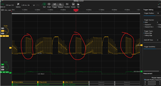
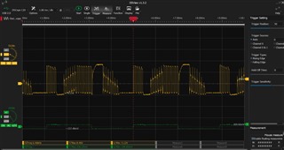
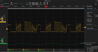
The output waveform is distorted; it's not a clean trapezoidal shape.
-
The motor heats up after a short time of operation and emits a noticeable high-pitched whine.
I'm suspecting there might be a misconfiguration in either hardware or software.
I'll be attaching the following for your reference:
-
Code that handles the hall sensor reading and commutation logic
-
Schematic of the custom board connected to the DRV8306
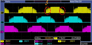
- Osciloscope images of the output phases and hall sensor readings.
I have tried a different motor with the same specs, and the noise goes away on a proprietary board that came with the motor. On both the only signals I'm providing from the MCU is the PWM and Enable signal.
Unfortunately I only have a two-channel osciloscope, so I couldn't see all the hall sensors and phases on the same image. It would be highly appreciated if someone could enlighten me on some possible causes. Thanks in advance for your help!
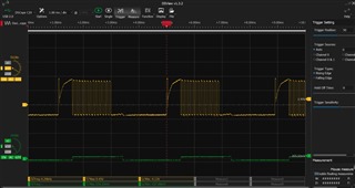
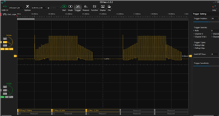
Phase A and hall A:
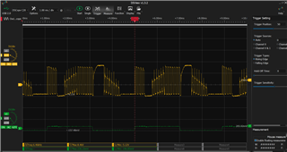
Phase B and hall B:
Phase C and hall C
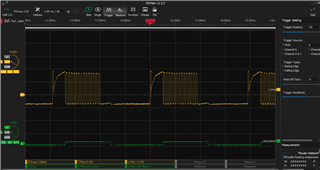
PWM Wave sent to the DRV: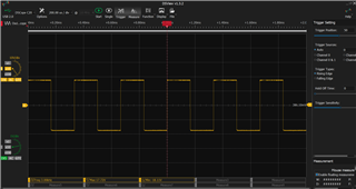
Code:
#include <msp430.h>
#include <stdbool.h>
#include <stdint.h>
#include <string.h>

#define ACLK		32768					// Frequência do ACLK 32,768 KHz
#define SMCLK		24000000				// Frequência do SMCLK 24 MHz


const uint8_t tb_div[][3] =	{	{1, 0, 0}, {2, 0, 1}, {3, 0, 2}, {4, 0, 3}, {5, 0, 4}, {6, 0, 5}, {7, 0, 6}, {8, 0, 7},
								{10, 1, 4}, {12, 1, 5}, {14, 1, 6}, {16, 1, 7}, {20, 2, 4}, {24, 2, 5}, {28, 2, 6},
								{32, 2, 7}, {40, 3, 4}, {48, 3, 5}, {56, 3, 6}, {64, 3, 7}, {0, 0, 0}};


bool blower_init(uint16_t pwm_frq);
void blower_set_dty (uint16_t dty);

int main(void)
{
    uint16_t flag = 0;
    uint16_t lng, dty = 5000,i=0;
    WDTCTL = WDTPW | WDTHOLD;               // Stop watchdog timer

    // S01 - Inicializa��o do Sistema: Clocks e PMM
    WDTCTL = WDTPW | WDTHOLD;                       // P�ra o Watchdog Timer
    FRCTL0 = FRCTLPW | NWAITS_2;                    // Configura 2 wait state para FRAM, pois MCLK ser� configurado em 24 MHz

    P2SEL0 &= ~(BIT7 | BIT6);                       // Configura P2.6 como XOUT e P2.7 como XIN
    P2SEL1 |= (BIT7 | BIT6);                        // P2.6:P2SELx = 10b, P2.7:P2SELx = 10b
    do{
        CSCTL7 &= ~(XT1OFFG | DCOFFG);              // Limpa flags de falha de XT1 e DCO
        SFRIFG1 &= ~OFIFG;                          // Limpa flag de interrup��o por falha de oscilador
    }while (SFRIFG1 & OFIFG);                       // Aguarda at� a flag de falha de oscilador ser limpa

    __bis_SR_register(SCG0);                        // Desabilita FLL

    CSCTL3 |= SELREF__XT1CLK;                       // Define XT1 como refer�ncia de clock para FLL
    CSCTL0 = 0;                                     // Inicializa CSCTL0.MOD = 00000b, pois o FLL ir� ajustar esses bits automaticamente
                                                    // Inicializa CSCTL0.DCO = 000000000b, pois o FLL ir� selecionar o tap do DCO automaticamente
    CSCTL1 &= ~(DCORSEL_7);                         // Primeiramente faz CSTL1.DCOR_SEL = 000b
    CSCTL1 |= DCORSEL_7;                            // Seta CSCTL1.DCOR_SEL = 110b: DCO = 24 MHz
    CSCTL2 = FLLD_0 + 731;                          // Configura CSCTL2.FLLD = 000b, seleciona divisor do FLL loop como fdcoclock + 1
                                                    // Configura CSCTL2.FLLN = 731, desta forma a frequencia do DCO ser� REFO = 32.768 Hz x (731 + 1) = 23.986.176 Hz ~ 24 MHz
    __delay_cycles(3);                              // Espera 3 ciclos de clock
    __bic_SR_register(SCG0);                        // Habilita FLL
    while (CSCTL7 & (FLLUNLOCK0 | FLLUNLOCK1));     // Espera FLL locked que ocorre quando CSCTL7.FLLUNLOCK = 00b

    CSCTL4 = SELA__XT1CLK | SELMS__DCOCLKDIV;       // Configura CSCTL4.SELA = 00b, escolhe XT1 como refer�ncia de clock para ACLK. Ent�o ACLK = 32.768 Hz
                                                    // Configura CSCTL4.SELMS = 000b, escolhe DCO como refer�ncia de clock para MCLK e SMCLK
    PM5CTL0 &= ~LOCKLPM5;                           // Desabilita o estado default de alta imp�d�ncia dos pinos de GPIO no power-on

    // S02 - Define regi�o da FRAM sem prote��o
    SYSCFG0 = 0xA51F;                               // SYSCFG0.FRWPPW = 0xA5:
                                                    // SYSCFG0.FRWPOA = 7: Seleciona 7 KB do in�cio da FRAM para DEV (1 KB) e DAT (6 KB) serem usados como RAM
                                                    // SYSCFG0.DFWP = 1:
                                                    // SYSCFG0.PFWP = 1

    P1DIR  = 0x00;                                  // Configura P1DIR conforme coment�rio acima
    P1SEL0 = 0xFF;                                  // Configura P1SEL0 conforme coment�rio acima
    P1SEL1 = 0xFF;                                  // Configura P1SEL1 conforme coment�rio acima
    P1OUT  = 0x00;                                  // Configura P1OUT conforme coment�rio acima
    P1REN  = 0x00;                                  // Configura P1REN conforme coment�rio acima

    P2DIR  = 0x3D;                                  // Configura P2DIR conforme coment�rio acima
    P2SEL0 = 0x01;                                  // Configura P2SEL0 conforme coment�rio acima
    P2SEL1 = 0xC0;                                  // Configura P2SEL1 conforme coment�rio acima
    P2OUT  = 0x00;                                  // Configura P2OUT conforme coment�rio acima
    P2REN  = 0x00;                                  // Configura P2REN conforme coment�rio acima

    P3DIR  = 0x11;                                  // Configura P3DIR conforme coment�rio acima
    P3SEL0 = 0xEE;                                  // Configura P3SEL0 conforme coment�rio acima
    P3SEL1 = 0xEE;                                  // Configura P3SEL1 conforme coment�rio acima
    P3OUT  = 0x00;                                  // Configura P3OUT conforme coment�rio acima
    P3REN  = 0x00;                                  // Configura P3REN conforme coment�rio acima

    P4DIR  = 0x01;                                  // Configura P4DIR conforme coment�rio acima
    P4SEL0 = 0x0C;                                  // Configura P4SEL0 conforme coment�rio acima
    P4SEL1 = 0x00;                                  // Configura P4SEL1 conforme coment�rio acima
    P4OUT  = 0x00;                                  // Configura P4OUT conforme coment�rio acima
    P4REN  = 0x00;                                  // Configura P4REN conforme coment�rio acima

    P5DIR  = 0x00;                                  // Configura P5DIR conforme coment�rio acima
    P5SEL0 = 0x03;                                  // Configura P5SEL0 conforme coment�rio acima
    P5SEL1 = 0x03;                                  // Configura P5SEL1 conforme coment�rio acima
    P5OUT  = 0x00;                                  // Configura P5OUT conforme coment�rio acima
    P5REN  = 0x00;                                  // Configura P5REN conforme coment�rio acima

    P6DIR  = 0x03;                                  // Configura P6DIR conforme coment�rio acima
    P6SEL0 = 0x03;                                  // Configura P6SEL0 conforme coment�rio acima
    P6SEL1 = 0x00;                                  // Configura P6SEL1 conforme coment�rio acima
    P6OUT  = 0x00;                                  // Configura P6OUT conforme coment�rio acima
    P6REN  = 0x00;                                  // Configura P6REN conforme coment�rio acima


    PM5CTL0 &= ~LOCKLPM5;                   // Disable the GPIO power-on default high-impedance mode
                                            // to activate previously configured port settings
    TB0CCTL0 = 0x0010;     // Habilita interrupção para CCR0
    TB0CCR0 = 32768 - 1;   // Define período de 32768 para que ocorra
    TB0CTL = 0x0110;       // TBCLGRP = 00b: Cada TBxCLn é armazenado independentemente (sem agrupamento);
                           // CNTL = 00b: Contador de 16 bits;
                           // TBSSEL = 01b: Utiliza ACLK = 32768 Hz como clock source;
                           // ID = 00b: Divide clock source por 1;
                           // MC = 01b: Modo de contagem UP;
                           // TBCLR = 0: Timer clear;
                           // TBIE = 0: Habilita interrupção;
                           // TBIFG = 0: Limpa interrupção pendente


    TB2CTL = 0x01E4;        // TBCLGRP = 00b: Cada TBxCLn é armazenado independentemente (sem agrupamento);
                            // CNTL = 00b: Contador de 16 bits;
                            // TBSSEL = 01b: Utiliza ACLK = 32768 Hz como clock source;
                            // ID = 11b: Divide clock source por 8, fazendo TB1CLK = ACLK / 8 = 4096Hz;
                            // MC = 10b: Modo de contagem CONTINUOS_MODE;
                            // TBCLR = 1: Timer clear;
                            // TBIE = 0: Desabilita interrupção;
                            // TBIFG = 0: Inrrelevante, pois não será utilizado interrupção para o timer
    TB2EX0 = 0x0003;        // TBIDEX = 011b: Divide o clock de 4096 Hz do divisor ID, por 4, obtendo um clock de 1024 Hz.


    TB3CTL = 0x02E6;       // TBCLGRP = 00b: Cada TBxCLn é armazenado independentemente (sem agrupamento);
                           // CNTL = 00b: Contador de 16 bits;
                           // TBSSEL = 10b: Utiliza SMCLK = 24 MHz como clock source;
                           // ID = 11b: Divide clock source por 8;
                           // MC = 10b: Modo de contagem Continuous;
                           // TBCLR = 1: Timer clear;
                           // TBIE = 1: Habilita interrupção;
                           // TBIFG = 0: Limpa interrupção pendente
   TB3EX0 = 0x0002;        // TBIDEX = 010b: Divide o clock de 3 MHz do divisor ID, por 3, obtendo um clock de 1 MHz.

    __enable_interrupt();

    blower_init(3000);


    while(1){
        blower_set_dty(dty);
        __delay_cycles(120000000);
        dty=0;
    }
}


/*
 * Fun��o que calcula a rota��o do motor para libera��o autom�tica
 * Par�metro de entrada:
 * uint16_t fgt_spd: velocidade de v�o, onde 1 = 0.1 Km/h
 * A fun��o retorna o valor de RPM que o motor deve girar para atender a taxa de aplica��o
 */
bool blower_init(uint16_t pwm_frq) {
    uint8_t i = 0;
    uint32_t hig, low;

    P2OUT |= BIT3; // Enable the blower control pin

    while (tb_div[i][0] != 0) { // Loop until the end of the tb_div table
        hig = SMCLK / tb_div[i][0]; // Calculate the highest frequency for the current divider
        low = hig / 65536;          // Calculate the lowest frequency for the current divider

        if (pwm_frq >= low) { // Check if the desired PWM frequency is within range
            uint32_t aux = hig / pwm_frq; // Calculate the period count for the desired frequency

            // Configure TB1
            TB1CCR0 = (uint16_t)aux;      // Set the period
            TB1CCTL1 = OUTMOD_7;          // Set output mode to Reset/Set
            TB1CCR1 = 0;                  // Initialize duty cycle to 0
            TB1CTL = TBCLR | TBSSEL__SMCLK | MC__UP | tb_div[i][1]; // Configure TB1CTL directly

            // Configure TB3
            TB3CCR0 = (uint16_t)aux;      // Set the period
            TB3CCTL1 = OUTMOD_7;          // Set output mode to Reset/Set
            TB3CCR1 = 0;                  // Initialize duty cycle to 0
            TB3CTL = TBCLR | TBSSEL__SMCLK | MC__UP | tb_div[i][1]; // Configure TB3CTL directly

            // Configure TB1EX0 and TB3EX0 for extended divider
            TB1EX0 = tb_div[i][2];
            TB3EX0 = tb_div[i][2];

            return true; // Successfully configured
        }

        i++; // Move to the next divider in the table
    }

    return false; // Failed to configure
}

void blower_set_dty (uint16_t dty){

	uint32_t aux;			// Vari�vel auxiliar para determinar valor da contagem do per�odo

	if (dty > 0){			// Verifica se o duty � positivo
		if (dty > 10000){	// Se sim, verifica se o duty � maior que 100%
			dty = 10000;	// Se for, limita em 100%
		}
		aux = dty;			// Carrega o valor do duty
		aux *= TB1CCR0;		// Multiplica pelo valor do per�odo
		aux /= 10000;		// Divide o resultado por 100%
		TB1CCR1 = (uint16_t) aux;	// Carrega o valor da contagem do per�odo
        aux = dty;          // Carrega o valor do duty
        aux *= TB3CCR0;     // Multiplica pelo valor do per�odo
        aux /= 10000;       // Divide o resultado por 100%
        TB3CCR1 = (uint16_t) aux;   // Carrega o valor da contagem do per�odo
		P4OUT |= BIT0;		// Habilita o blower
		P3OUT &= ~BIT0;
	}
	else{					// Para o motor
		TB1CCR1 = 0;		// Configura o duty cycle = 0
		TB3CCR1 = 0;
		P4OUT &= ~BIT0;			// Desabilita o blower
		P3OUT |= BIT0;         // Desabilita o blower
	}
}
Video of the noise:
Board Diagram: