This thread has been locked.

If you have a related question, please click the "Ask a related question" button in the top right corner. The newly created question will be automatically linked to this question.

Failure of DRV8302 Pre-Driver

Other Parts Discussed in Thread: DRV8302, DRV8332, DRV8301

Hi,

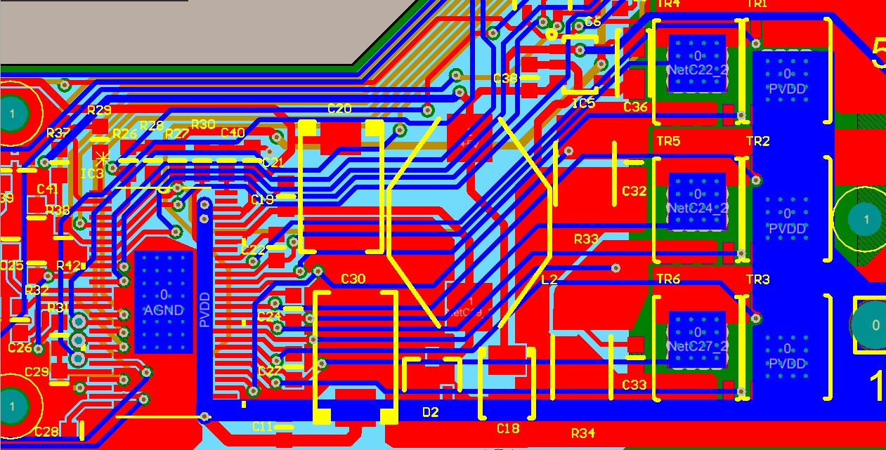
I've been trying to develop a design using the DRV8302 motor pre-driver and have had some success with the suggested schematic. I've run our brushless dc motor under load at around 30V PVDD. However, I've also had a couple of failures and am now trying to understand what may have been over-stressed, and what could have caused this. The failure seems to have occurred when the motor has stopped abruptly, perhaps suggesting a rate of change problem? Subsequently testing the failed boards with a PVDD of around 8V, I still appear to be able to talk to the chip, but at the point at which I turn on the gate drive, the FAULT line is asserted, the circuit takes around 180mA, and the GVDD supply is only perhaps 4V. Obviously, I need to know what to do to fully protect the circuit, but there are no clues from the data sheet.


Kind regards,


John

  • Hi John,

    Looking through other forum posts, the TI EVM can handle 60V and 60A. Please refer to post http://e2e.ti.com/support/applications/motor_drivers/f/38/p/227363/800335.aspx#800335 for details.

    There are a few common problems that have been seen when developing new boards.

    Are you following the schematic on page 17 of the datasheet or the EVM schematic as a guide? Please be sure to add a bulk capacitor (470uF on the datasheet schematic), and smaller filter capacitors (4.7uF and .1uF) close to PVDDx.

    Also, it is very important to connect the grounds together (especially pin 57, the power pad ground).

    If you are still having problems, can you send the schematic of your design?

  • Thanks for your suggestions. At present, because of space constraints, I'm only using a 100uF bulk capacitor on PVDD, but with the recommended local de-coupling close to the chip. However, I suspect this is not the problem, as the buck converter seems to survive ok.

    is it likely that I've got over-voltage spikes on the phase outputs (i.e. the motor windings), as these are input by the chip in order to measure over current? If you think this is likely, would it help to add TVSs to these outputs to try to clamp any transients?


  • Hi John,

    I apologize for the many questions.

    Just to confirm, you are running the motor at 30VDC. Correct?

    Can you describe the scenario where you are stopping the motor? How much current is flowing through the motor? What are the predrivers set to when this occurs?

    Have you measured the spikes on PVDD when this event occurs?

    When GVDD is only 4V, have you removed the FETs to confirm that it is the charge pump loading failing and not the FETs?

    Any scope captures, schematics, and layouts that you can share would be beneficial. Thanks.


  • Hi Rick,

    Although the failures occurred when I was running the motor with a PVDD of about 31V, I will be running with a voltage of up to 40V from a 36V battery. Unfortunately I don't really have any recorded data for when the failures occurred because I was wasn't really expecting it - I only have a very few prototypes I'm working on, so any failure is a real pain. However, there are some further clues:

    • First of all, I know it's the chip that's failed because I've now changed three of them and the boards work again. The FETs appear to be undamaged.
    • There appears to be some ringing on the outputs. I've improved this by adding small resistors and reverse diodes in series with the gates.
    • Using a power supply, I can get large over-voltages on the outputs (up to 2 x PVDD, as expected - it's a motor, after all!), but they should be within the maximum of the chip. With a battery, these voltage excursions will be very much reduced. They're also reduced if I control deceleration properly.

    Another possible clue is that when the motor is running at no load, I sometimes observe some cycle-by-cycle current limiting. This doesn't appear to be a problem at load.

    I suspect that the problem is a combination of normal over-voltage (motor generation) and some ringing as well. Hence my thought to add some over-voltage protection.

    Thanks, John


  • Hi Rick,

    Any further thoughts? I don't believe I have a definitive cure yet for the problems, as I've had another failure on a modified pcb. I've looked at my software and believe that the problems could have been caused by some abrupt reversals in speed demand, but why would that damage the chip?

    By the way, this design was an upgrade from a previous version that used the DRV8332. This had proved to be quite robust, but doesn't give enough current for the present application, which requires in excess of 10A.

    Hoping you may be able to look at this again soon,

    Regards,

    John

  • Hi John,

    Can we see a snapshot of the schematic/layout around the DRV part and FETs? Layout is crucial for this part especially when trying to utilize higher currents.

    Please see this post about the DRV8301 (sister part)

    http://e2e.ti.com/support/applications/motor_drivers/f/38/p/279474/976444.aspx#976444

  • Hi Nicholas,

    I'm sure pcb layout is likely to be an issue, I believe that the cct is as per the data sheet, but there seem to be scant details about the layout, so thanks for the post you've copied me. With regard to the layout, I should mention that it is intended that the pcb will be in thermal contact with a heat spreader beneath the board, as it's in an enclosed space and could have to operate at elevated temperatures. The board shape is also governed to a certain extent by the structure in which it sits. Note also that the light blue layer is connected to AGND

    Thanks,

    John


    7418.Outputs.PDF


  • John,

    We are actually in the process of appending a layout guide to the datasheet. I'll give your design a lookover and see if anything looks suspicous.

  • John,

    One issue that sticks out immediately to me is the GND return path to PPAD for C20 and C30. It look as if this copper fill is isolated only returning back towards the FETs. You may also want to utilize kelvin, differential traces for the op-amp feedbacks from the sense resistors. GND bounce and switching noise is going to affect those readings.

    Also, what is the purpose of the AGND layer? It is difficult to tell where it connects and it does not appear that the other GND fills connect to it.

    I am going to post the note we are working on, this is in no way official yet. The design in the note is a compact 2-layer board.

    4341.DRV8301-2_Layout_Recs.pdf