Hi all,
I am developing a new board equipped with two DRV8412.
Each DRV is configured in Dual full bridge mode with OC latching.
Power supply voltages are set with the following values:
PVDD = +24Vdc properly bypassed
GVDD = +12Vdc obtained from a linear regulator supplyed with the same +24Vdc that is connected to PVDD
and properly bypassed.
Each full bridge drives a 750uH inductive load (the full board drives 4 inductive loads).
The load current control is based on a standard chopping technique; PWM frequency is set to 31KHz.
About the PCB layout, it has been developed following the guidelines present on datasheet. Both DRV8412 and their
circuitry have been placed close to the output connectors.
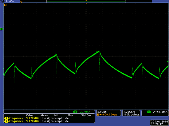
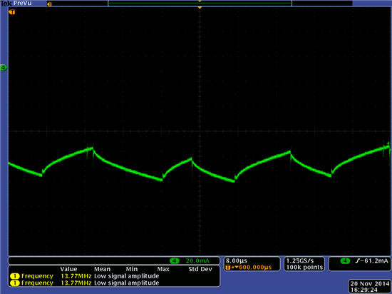
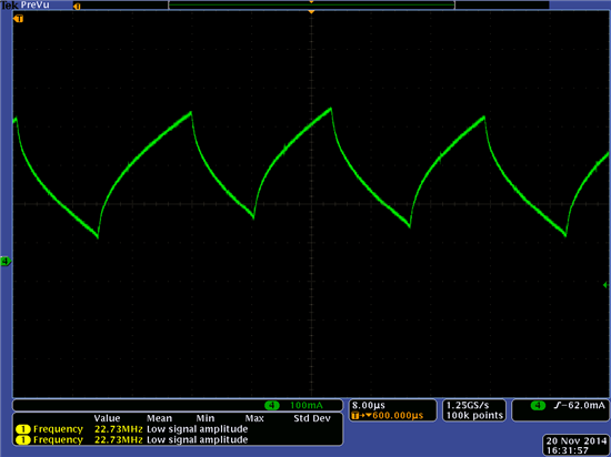
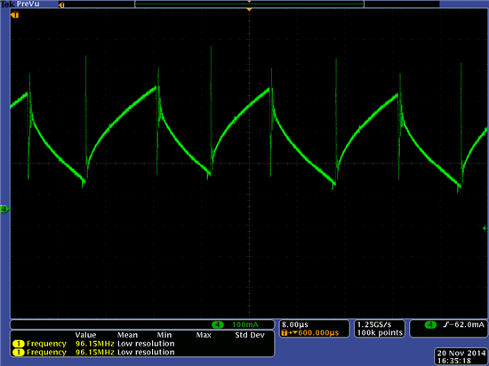
The problem I am seeing is that from bridge AB i get a clean current waveform; from bridge CD I get a "dirty" current waveform, as illustrated in the pictures attached. This happens on both the DRV8412 on the same board and on different boards.
Image1: current waveform obtained from bridge AB (on the left, the full waveform, on the right a detail).
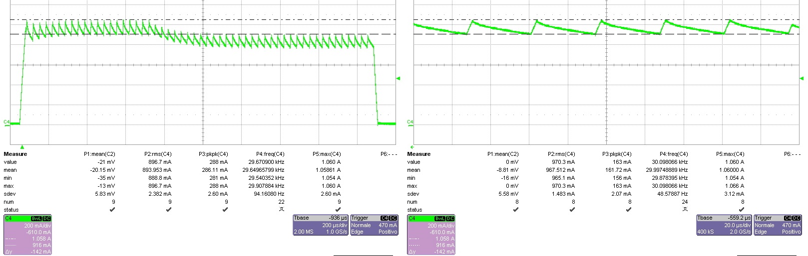
Image2: current waveform obtained from bridge CD.

Can anyone suggest me where is the source of this behaviour and give me a suggestion on how to reduce or eliminate it?
Thanks a lot,
Sergio