Other Parts Discussed in Thread: DRV8301, MOTORWARE, CSD19532Q5B
Hi,
I just soldered my own designed controller board. I based it on the DRV8353 EV and DRV8301-69 kit. So I'm using F28069F processor and DRV8353 driver, because my battery voltage has a maximum of about 58V.
So, what have I done so far?
- I did all instapsin-FOC labs with DRV8301-69 EV kit
- I did the modified lab 05b with DRV8353 EVM - but it is somehow current limited, see below.
- And I prefere to use the 11e project as a base, because I need current control and I need to startup with Hall sensors at low rpm and need then to switch to FAST. I tried without HALL, but it is not a good experience under load, starting from zero...
Now coming to my own board. I have done the following:
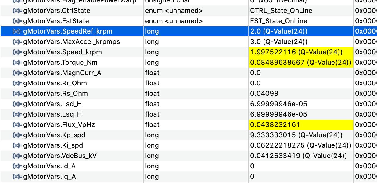
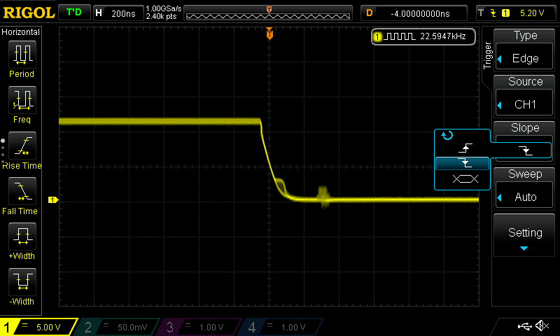
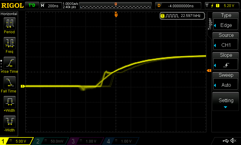
- Modified the Lab05b_drv8353 to meet my custom board and F28069F and it is running, but somehow power limited. I can set for example 2000 rpm, but as soon as I put load on it, it drops down to 1200 rpm. Current on power supply side is then about 2A. No matter what I increase in request in gMotorVars.SpeedRef_krpm. Any idea why is this ?When motor is stopped, I see sometime jumps up to 9000/4000 in gMotorVars.Speed_krpm. I noticed a jump in voltage measurement of phase C. It goes from 0.0 sometime up to -2.0... But ADC value in ADCResult does not jump... I did check back with DRV8353H EV kit, and it has the same behavior... motor is running on 2000 rpm, I put load on it, current goes up to 4 amps, and then motor is slowing down to about 1200 rpm and 2A from power supply. Power supply can definitely deliver more power than that. Is here some limitation active in DRV8353 or something ? my USER_MOTOR_MAX_CURRENT is set to 14.0 A.
- And on project 11e, nothing is really working... When I only enable the Identify and enableSys Flags, in hall mode motor starts turning backwards (about 1000 - 2000 rpm), but FS_IQ_ref is 0.0 and in current control mode, motor does not start, just a short try in turn of the motor, followed by complete shutdown --> hitting pause on debugging shows message: break at adress xxx with no debug information available...
So to summarize:
So, from my point of view, my modified 05b is more working, but 11e is more like the featureset I need in the end (current control and HALL startup)
My questions:
1) Do you have an idea, why 05b project is somehow current limited ?
2) Do you have an idea, what is wrong in 11e for my custom board ?
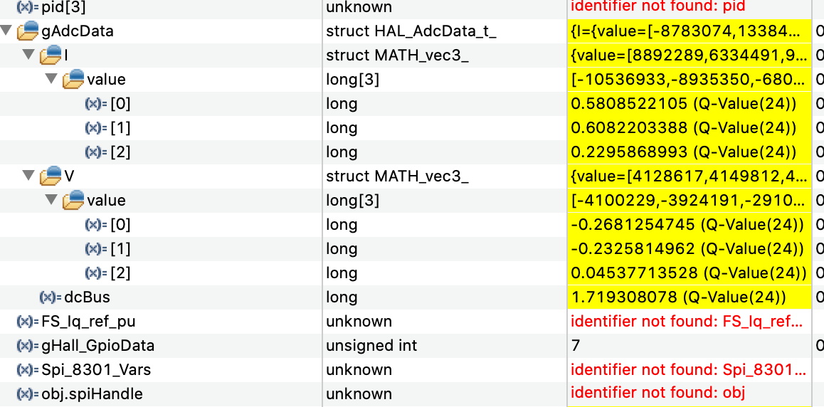
3) What I can imagine: I'm not sure, how to get/calculate the I_offsets and V_offsets. They are quite different in the projects for drv8353 and drv8301 ---> How Do I get these values?
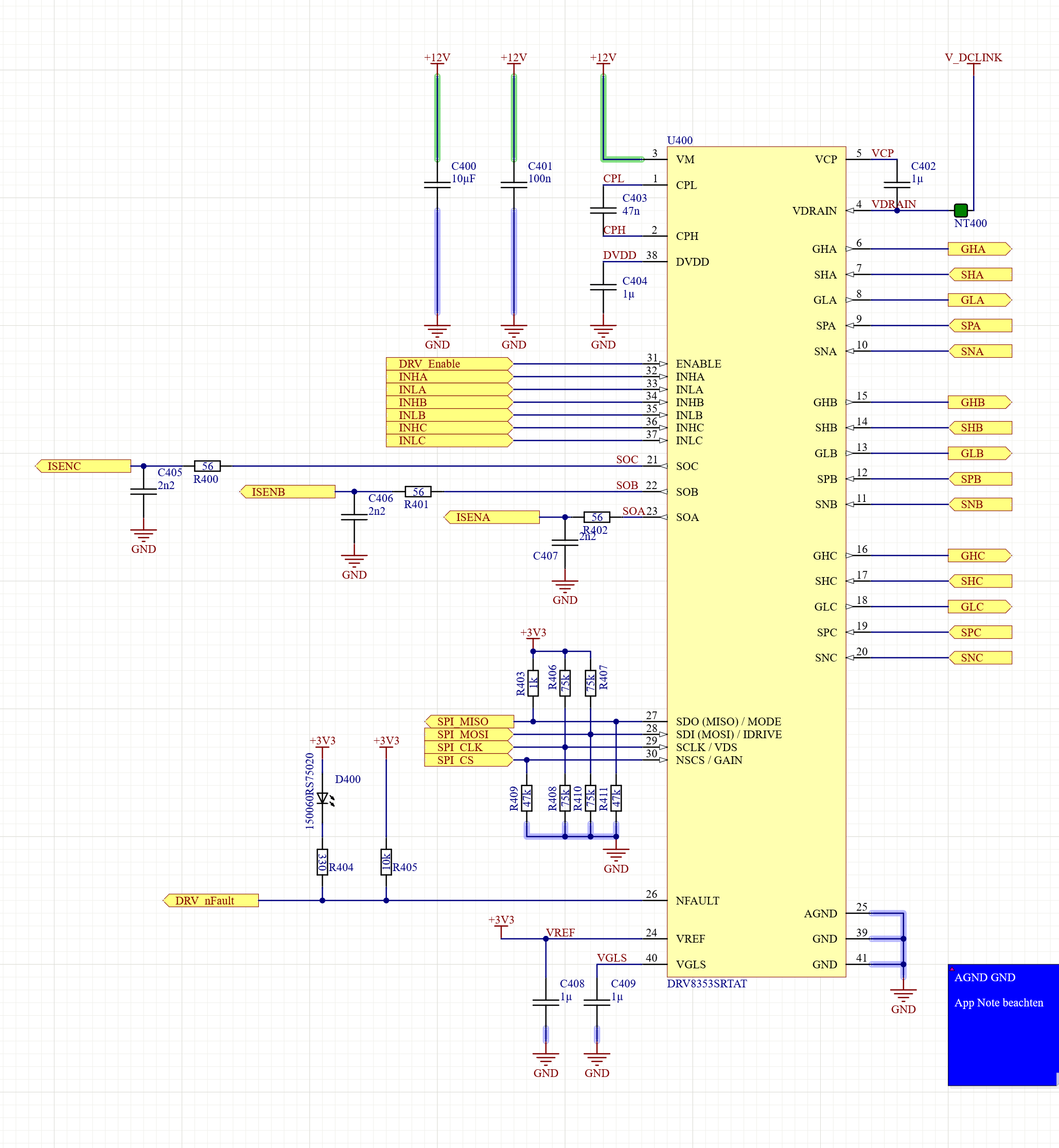
4) current and voltage scale factors should I did calculate and change the approbiate values in user.h. I attach my user.h, and my schematic.
0871.user.hI'm using the same files for 05b and 11e (Hal, user.h, drv8353 etc.)

proj_lab05b_drv8353_modified.rtf
/* --COPYRIGHT--,BSD
 * Copyright (c) 2015, Texas Instruments Incorporated
 * All rights reserved.
 *
 * Redistribution and use in source and binary forms, with or without
 * modification, are permitted provided that the following conditions
 * are met:
 *
 * *  Redistributions of source code must retain the above copyright
 *    notice, this list of conditions and the following disclaimer.
 *
 * *  Redistributions in binary form must reproduce the above copyright
 *    notice, this list of conditions and the following disclaimer in the
 *    documentation and/or other materials provided with the distribution.
 *
 * *  Neither the name of Texas Instruments Incorporated nor the names of
 *    its contributors may be used to endorse or promote products derived
 *    from this software without specific prior written permission.
 *
 * THIS SOFTWARE IS PROVIDED BY THE COPYRIGHT HOLDERS AND CONTRIBUTORS "AS IS"
 * AND ANY EXPRESS OR IMPLIED WARRANTIES, INCLUDING, BUT NOT LIMITED TO,
 * THE IMPLIED WARRANTIES OF MERCHANTABILITY AND FITNESS FOR A PARTICULAR
 * PURPOSE ARE DISCLAIMED. IN NO EVENT SHALL THE COPYRIGHT OWNER OR
 * CONTRIBUTORS BE LIABLE FOR ANY DIRECT, INDIRECT, INCIDENTAL, SPECIAL,
 * EXEMPLARY, OR CONSEQUENTIAL DAMAGES (INCLUDING, BUT NOT LIMITED TO,
 * PROCUREMENT OF SUBSTITUTE GOODS OR SERVICES; LOSS OF USE, DATA, OR PROFITS;
 * OR BUSINESS INTERRUPTION) HOWEVER CAUSED AND ON ANY THEORY OF LIABILITY,
 * WHETHER IN CONTRACT, STRICT LIABILITY, OR TORT (INCLUDING NEGLIGENCE OR
 * OTHERWISE) ARISING IN ANY WAY OUT OF THE USE OF THIS SOFTWARE,
 * EVEN IF ADVISED OF THE POSSIBILITY OF SUCH DAMAGE.
 * --/COPYRIGHT--*/
//! \file   drivers/drvic/drv8305/src/32b/f28x/f2806x/drv8353.c
//! \brief  Contains the various functions related to the DRV8353 object
//!
//! (C) Copyright 2015, Texas Instruments, Inc.
//  MW_INSTALL_DIR
//  ${PROJECT_LOC}\..\..\..\..\..\..\..\..\..\..
//
// **************************************************************************
// the includes

#include <math.h>


// **************************************************************************
// drivers
#include "sw/drivers/drvic/drv8353/src/32b/f28x/f2802x/drv8353.h"


// **************************************************************************
// modules


// **************************************************************************
// platforms


// **************************************************************************
// the defines


// **************************************************************************
// the globals


// **************************************************************************
// the function prototypes


DRV8353_Handle DRV8353_init(void *pMemory,const size_t numBytes)
{
  DRV8353_Handle handle;

  if(numBytes < sizeof(DRV8353_Obj))
    return((DRV8353_Handle)NULL);

  // assign the handle
  handle = (DRV8353_Handle)pMemory;

  DRV8353_resetRxTimeout(handle);
  DRV8353_resetEnableTimeout(handle);

  return(handle);
} // end of DRV8353_init() function


void DRV8353_enable(DRV8353_Handle handle)
{
  DRV8353_Obj *obj = (DRV8353_Obj *)handle;
  static volatile uint16_t enableWaitTimeOut;
  uint16_t n = 0;

  // Enable the DRV8353
  GPIO_setHigh(obj->gpioHandle,obj->gpioNumber);


  enableWaitTimeOut = 0;
#ifdef DRV8353_SPI
  if(gDeviceVariant)
  {
  // Make sure the FAULT bit is not set during startup
  while(((DRV8353_readSpi(handle, Address_Status_0) & DRV8353_STATUS00_FAULT_BITS) != 0) && (enableWaitTimeOut < 1000))
  {
      if (++enableWaitTimeOut > 999)
      {
          obj->enableTimeOut = true;
      }
  }
  }
else
#endif
{
  while(enableWaitTimeOut < 1000)
   {
       if (++enableWaitTimeOut > 999)
       {
           obj->enableTimeOut = true;
       }
   }
}
  // Wait for the DRV8353 to go through start up sequence
  for(n=0;n<0xffff;n++)
    asm(" NOP");

  return;
} // end of DRV8353_enable() function

#ifdef DRV8353_SPI
DRV8353_CTRL03_PeakSourCurHS_e DRV8353_getPeakSourCurHS(DRV8353_Handle handle)
{
  uint16_t data;

  // read data
  data = DRV8353_readSpi(handle,Address_Control_3);

  // mask the bits
  data &= DRV8353_CTRL03_IDRIVEP_HS_BITS;

  return((DRV8353_CTRL03_PeakSourCurHS_e)data);
} // end of DRV8353_getPeakSourCurHS function


DRV8353_CTRL03_PeakSinkCurHS_e DRV8353_getPeakSinkCurHS(DRV8353_Handle handle)
{
  uint16_t data;

  // read data
  data = DRV8353_readSpi(handle,Address_Control_3);

  // mask the bits
  data &= DRV8353_CTRL03_IDRIVEN_HS_BITS;

  return((DRV8353_CTRL03_PeakSinkCurHS_e)data);
} // end of DRV8353_getPeakSinkCurHS function


DRV8353_CTRL04_PeakTime_e DRV8353_getPeakSourTime(DRV8353_Handle handle)
{
  uint16_t data;

  // read data
  data = DRV8353_readSpi(handle,Address_Control_4);

  // mask the bits
  data &= DRV8353_CTRL04_TDRIVE_BITS;

  return((DRV8353_CTRL04_PeakTime_e)data);
} // end of DRV8353_getPeakSourTime function


DRV8353_CTRL04_PeakSourCurLS_e DRV8353_getPeakSourCurLS(DRV8353_Handle handle)
{
  uint16_t data;

  // read data
  data = DRV8353_readSpi(handle,Address_Control_4);

  // mask the bits
  data &= DRV8353_CTRL04_IDRIVEP_LS_BITS;

  return((DRV8353_CTRL04_PeakSourCurLS_e)data);
} // end of DRV8353_getPeakSourCurLS function


DRV8353_CTRL04_PeakSinkCurLS_e DRV8353_getPeakSinkCurLS(DRV8353_Handle handle)
{
  uint16_t data;

  // read data
  data = DRV8353_readSpi(handle,Address_Control_4);

  // mask the bits
  data &= DRV8353_CTRL04_IDRIVEN_LS_BITS;

  return((DRV8353_CTRL04_PeakSinkCurLS_e)data);
} // end of DRV8353_getPeakSinkCurLS function
#endif
/*
DRV8353_CTRL04_PeakSinkTime_e DRV8353_getPeakSinkTime(DRV8353_Handle handle)
{
  uint16_t data;

  // read data
  data = DRV8353_readSpi(handle,Address_Control_4);

  // mask the bits
  data &= DRV8353_CTRL04_TDRIVE_BITS;

  return((DRV8353_CTRL04_PeakSinkTime_e)data);
} // end of DRV8353_getPeakSinkTime function
*/
#ifdef DRV8353_SPI
DRV8353_CTRL05_OcpDeg_e DRV8353_getVDSDeglitch(DRV8353_Handle handle)
{
  uint16_t data;

  // read data
  data = DRV8353_readSpi(handle,Address_Control_5);

  // mask the bits
  data &= DRV8353_CTRL05_OCP_DEG_BITS;

  return((DRV8353_CTRL05_OcpDeg_e)data);
} // end of DRV8353_getVDSDeglitch function

/*
DRV8305_CTRL07_VDSBlanking_e DRV8353_getVDSBlanking(DRV8353_Handle handle)
{
  uint16_t data;

  // read data
  data = DRV8353_readSpi(handle,Address_Control_7);

  // mask the bits
  data &= DRV8305_CTRL07_TBLANK_BITS;

  return((DRV8305_CTRL07_VDSBlanking_e)data);
} // end of DRV8305_getVDSBlanking function
*/

DRV8353_CTRL05_DeadTime_e DRV8353_getDeadTime(DRV8353_Handle handle)
{
  uint16_t data;

  // read data
  data = DRV8353_readSpi(handle,Address_Control_5);

  // mask the bits
  data &= DRV8353_CTRL05_DEAD_TIME_BITS;

  return((DRV8353_CTRL05_DeadTime_e)data);
} // end of DRV8353_getDeadTime function


DRV8353_CTRL02_PwmMode_e DRV8353_getPwmMode(DRV8353_Handle handle)
{
  uint16_t data;

  // read data
  data = DRV8353_readSpi(handle,Address_Control_2);

  // mask the bits
  data &= DRV8353_CTRL02_PWM_MODE_BITS;

  return((DRV8353_CTRL02_PwmMode_e)data);
} // end of DRV8353_getPwmMode function

/*
DRV8305_CTRL07_CommOption_e DRV8353_getCommOption(DRV8353_Handle handle)
{
  uint16_t data;

  // read data
  data = DRV8305_readSpi(handle,Address_Control_7);

  // mask the bits
  data &= DRV8305_CTRL07_COMM_OPT_BITS;

  return((DRV8305_CTRL07_CommOption_e)data);
} // end of DRV8305_getCommOption function


DRV8305_CTRL09_WatchDelay_e DRV8353_getWatchDelay(DRV8353_Handle handle)
{
  uint16_t data;

  // read data
  data = DRV8305_readSpi(handle,Address_Control_9);

  // mask the bits
  data &= DRV8305_CTRL09_WD_DLY_BITS;

  return((DRV8305_CTRL09_WatchDelay_e)data);
} // end of DRV8305_getWatchDelay function


DRV8305_CTRL0A_CSGain1_e DRV8353_getCSGain1(DRV8353_Handle handle)
{
  uint16_t data;

  // read data
  data = DRV8305_readSpi(handle,Address_Control_A);

  // mask the bits
  data &= DRV8305_CTRL0A_GAIN_CS1_BITS;

  return((DRV8305_CTRL0A_CSGain1_e)data);
} // end of DRV8305_getCSGain1 function


DRV8305_CTRL0A_CSGain2_e DRV8353_getCSGain2(DRV8353_Handle handle)
{
  uint16_t data;

  // read data
  data = DRV8305_readSpi(handle,Address_Control_A);

  // mask the bits
  data &= DRV8305_CTRL0A_GAIN_CS2_BITS;

  return((DRV8305_CTRL0A_CSGain2_e)data);
} // end of DRV8305_getCSGain2 function


DRV8305_CTRL0A_CSGain3_e DRV8353_getCSGain3(DRV8353_Handle handle)
{
  uint16_t data;

  // read data
  data = DRV8305_readSpi(handle,Address_Control_A);

  // mask the bits
  data &= DRV8305_CTRL0A_GAIN_CS3_BITS;

  return((DRV8305_CTRL0A_CSGain3_e)data);
} // end of DRV8305_getCSGain3 function


DRV8305_CTRL0A_CSBlank_e DRV8353_getCSBlank(DRV8353_Handle handle)
{
  uint16_t data;

  // read data
  data = DRV8305_readSpi(handle,Address_Control_A);

  // mask the bits
  data &= DRV8305_CTRL0A_CS_BLANK_BITS;

  return((DRV8305_CTRL0A_CSBlank_e)data);
} // end of DRV8305_getCSBlank function


DRV8305_CTRL0A_DcCalMode_e DRV8353_getDcCalMode(DRV8353_Handle handle,const DRV8305_ShuntAmpNumber_e ampNumber)
{
  uint16_t data;

  // read data
  data = DRV8305_readSpi(handle,Address_Control_A);

  // mask the bits
  if(ampNumber == ShuntAmpNumber_1)
    {
      data &= DRV8305_CTRL0A_DC_CAL_CH1_BITS;
    }
  else if(ampNumber == ShuntAmpNumber_2)
    {
      data &= DRV8305_CTRL0A_DC_CAL_CH2_BITS;
    }
  else if(ampNumber == ShuntAmpNumber_3)
    {
      data &= DRV8305_CTRL0A_DC_CAL_CH3_BITS;
    }

  return((DRV8305_CTRL0A_DcCalMode_e)data);
} // end of DRV8305_getDcCalMode() function


DRV8305_CTRL0B_VregUvLevel_e DRV8353_getVregUvLevel(DRV8353_Handle handle)
{
  uint16_t data;

  // read data
  data = DRV8305_readSpi(handle,Address_Control_B);

  // mask the bits
  data &= DRV8305_CTRL0B_VREG_UV_LEVEL_BITS;

  return((DRV8305_CTRL0B_VregUvLevel_e)data);
} // end of DRV8305_getVregUvLevel function


DRV8305_CTRL0B_SleepDelay_e DRV8353_getSleepDelay(DRV8353_Handle handle)
{
  uint16_t data;

  // read data
  data = DRV8305_readSpi(handle,Address_Control_B);

  // mask the bits
  data &= DRV8305_CTRL0B_SLP_DLY_BITS;

  return((DRV8305_CTRL0B_SleepDelay_e)data);
} // end of DRV8305_getSleepDelay function


DRV8305_CTRL0B_VrefScaling_e DRV8353_getVrefScaling(DRV8353_Handle handle)
{
  uint16_t data;

  // read data
  data = DRV8305_readSpi(handle,Address_Control_B);

  // mask the bits
  data &= DRV8305_CTRL0B_VREF_SCALING_BITS;

  return((DRV8305_CTRL0B_VrefScaling_e)data);
} // end of DRV8305_getVrefScaling function


DRV8305_CTRL0C_VDSMode_e DRV8353_getVDSMode(DRV8353_Handle handle)
{
  uint16_t data;

  // read data
  data = DRV8305_readSpi(handle,Address_Control_C);

  // mask the bits
  data &= DRV8305_CTRL0C_VDS_MODE_BITS;

  return((DRV8305_CTRL0C_VDSMode_e)data);
} // end of DRV8305_getVDSMode function


DRV8305_CTRL0C_VDSLevel_e DRV8353_getVDSLevel(DRV8353_Handle handle)
{
  uint16_t data;

  // read data
  data = DRV8305_readSpi(handle,Address_Control_C);

  // mask the bits
  data &= DRV8305_CTRL0C_VDS_LEVEL_BITS;

  return((DRV8305_CTRL0C_VDSLevel_e)data);
} // end of DRV8305_getVDSLevel function
*/

void DRV8353_setSpiHandle(DRV8353_Handle handle,SPI_Handle spiHandle)
{
  DRV8353_Obj *obj = (DRV8353_Obj *)handle;

  // initialize the serial peripheral interface object
  obj->spiHandle = spiHandle;

  return;
} // end of DRV8353_setSpiHandle() function
#endif

void DRV8353_setGpioHandle(DRV8353_Handle handle,GPIO_Handle gpioHandle)
{
  DRV8353_Obj *obj = (DRV8353_Obj *)handle;

  // initialize the gpio interface object
  obj->gpioHandle = gpioHandle;

  return;
} // end of DRV8353_setGpioHandle() function


void DRV8353_setGpioNumber(DRV8353_Handle handle,GPIO_Number_e gpioNumber)
{
  DRV8353_Obj *obj = (DRV8353_Obj *)handle;

  // initialize the gpio interface object
  obj->gpioNumber = gpioNumber;

  return;
} // end of DRV8353_setGpioNumber() function

/*
void DRV8305_setPeakSourCurHS(DRV8353_Handle handle,const DRV8305_CTRL05_PeakSourCurHS_e level)
{
  uint16_t data;

  // read data
  data = DRV8305_readSpi(handle,Address_Control_5);

  // clear the bits
  data &= (~DRV8305_CTRL05_IDRIVEP_HS_BITS);

  // set the bits
  data |= level;

  // write the data
  DRV8305_writeSpi(handle,Address_Control_5,data);

  return;
} // end of DRV8305_setPeakSourCurHS() function


void DRV8305_setPeakSinkCurHS(DRV8353_Handle handle,const DRV8305_CTRL05_PeakSinkCurHS_e level)
{
  uint16_t data;

  // read data
  data = DRV8305_readSpi(handle,Address_Control_5);

  // clear the bits
  data &= (~DRV8305_CTRL05_IDRIVEN_HS_BITS);

  // set the bits
  data |= level;

  // write the data
  DRV8305_writeSpi(handle,Address_Control_5,data);

  return;
} // end of DRV8305_setPeakSinkCurHS() function


void DRV8305_setPeakSourTime(DRV8353_Handle handle,const DRV8305_CTRL05_PeakSourTime_e time)
{
  uint16_t data;

  // read data
  data = DRV8305_readSpi(handle,Address_Control_5);

  // clear the bits
  data &= (~DRV8305_CTRL05_TDRIVEN_BITS);

  // set the bits
  data |= time;

  // write the data
  DRV8305_writeSpi(handle,Address_Control_5,data);

  return;
} // end of DRV8305_setPeakSourTime() function


void DRV8305_setPeakSinkCurLS(DRV8353_Handle handle,const DRV8305_CTRL06_PeakSinkCurLS_e level)
{
  uint16_t data;

  // read data
  data = DRV8305_readSpi(handle,Address_Control_6);

  // clear the bits
  data &= (~DRV8305_CTRL06_IDRIVEP_LS_BITS);

  // set the bits
  data |= level;

  // write the data
  DRV8305_writeSpi(handle,Address_Control_6,data);

  return;
} // end of DRV8305_setPeakSinkCurLS() function


void DRV8305_setPeakSinkTime(DRV8353_Handle handle,const DRV8305_CTRL06_PeakSinkTime_e time)
{
  uint16_t data;

  // read data
  data = DRV8305_readSpi(handle,Address_Control_6);

  // clear the bits
  data &= (~DRV8305_CTRL06_TDRIVEP_BITS);

  // set the bits
  data |= time;

  // write the data
  DRV8305_writeSpi(handle,Address_Control_6,data);

  return;
} // end of DRV8305_setPeakSinkTime() function


void DRV8305_setVDSDeglitch(DRV8353_Handle handle,const DRV8305_CTRL07_VDSDeglitch_e time)
{
  uint16_t data;

  // read data
  data = DRV8305_readSpi(handle,Address_Control_7);

  // clear the bits
  data &= (~DRV8305_CTRL07_TVDS_BITS);

  // set the bits
  data |= time;

  // write the data
  DRV8305_writeSpi(handle,Address_Control_7,data);

  return;
} // end of DRV8305_setVDSDeglitch() function


void DRV8305_setVDSBlanking(DRV8353_Handle handle,const DRV8305_CTRL07_VDSBlanking_e time)
{
  uint16_t data;

  // read data
  data = DRV8305_readSpi(handle,Address_Control_7);

  // clear the bits
  data &= (~DRV8305_CTRL07_TBLANK_BITS);

  // set the bits
  data |= time;

  // write the data
  DRV8305_writeSpi(handle,Address_Control_7,data);

  return;
} // end of DRV8305_setVDSBlanking() function


void DRV8305_setDeadTime(DRV8353_Handle handle,const DRV8305_CTRL07_DeadTime_e time)
{
  uint16_t data;

  // read data
  data = DRV8305_readSpi(handle,Address_Control_7);

  // clear the bits
  data &= (~DRV8305_CTRL07_DEAD_TIME_BITS);

  // set the bits
  data |= time;

  // write the data
  DRV8305_writeSpi(handle,Address_Control_7,data);

  return;
} // end of DRV8305_setDeadTime() function


void DRV8305_setPwmMode(DRV8353_Handle handle,const DRV8305_CTRL07_PwmMode_e mode)
{
  uint16_t data;

  // read data
  data = DRV8305_readSpi(handle,Address_Control_7);

  // clear the bits
  data &= (~DRV8305_CTRL07_PWM_MODE_BITS);

  // set the bits
  data |= mode;

  // write the data
  DRV8305_writeSpi(handle,Address_Control_7,data);

  return;
} // end of DRV8305_setPwmMode() function


void DRV8305_setCommOption(DRV8353_Handle handle,const DRV8305_CTRL07_CommOption_e mode)
{
  uint16_t data;

  // read data
  data = DRV8305_readSpi(handle,Address_Control_7);

  // clear the bits
  data &= (~DRV8305_CTRL07_COMM_OPT_BITS);

  // set the bits
  data |= mode;

  // write the data
  DRV8305_writeSpi(handle,Address_Control_7,data);

  return;
} // end of DRV8305_setCommOption() function


void DRV8305_setWatchDelay(DRV8353_Handle handle,const DRV8305_CTRL09_WatchDelay_e time)
{
  uint16_t data;

  // read data
  data = DRV8305_readSpi(handle,Address_Control_9);

  // clear the bits
  data &= (~DRV8305_CTRL09_WD_DLY_BITS);

  // set the bits
  data |= time;

  // write the data
  DRV8305_writeSpi(handle,Address_Control_9,data);

  return;
} // end of DRV8305_setWatchDelay() function


void DRV8305_setCSGain1(DRV8353_Handle handle,const DRV8305_CTRL0A_CSGain1_e gain)
{
  uint16_t data;

  // read data
  data = DRV8305_readSpi(handle,Address_Control_A);

  // clear the bits
  data &= (~DRV8305_CTRL0A_GAIN_CS1_BITS);

  // set the bits
  data |= gain;

  // write the data
  DRV8305_writeSpi(handle,Address_Control_A,data);

  return;
} // end of DRV8305_setCSGain1() function


void DRV8305_setCSGain2(DRV8353_Handle handle,const DRV8305_CTRL0A_CSGain2_e gain)
{
  uint16_t data;

  // read data
  data = DRV8305_readSpi(handle,Address_Control_A);

  // clear the bits
  data &= (~DRV8305_CTRL0A_GAIN_CS2_BITS);

  // set the bits
  data |= gain;

  // write the data
  DRV8305_writeSpi(handle,Address_Control_A,data);

  return;
} // end of DRV8305_setCSGain2() function


void DRV8305_setCSGain3(DRV8353_Handle handle,const DRV8305_CTRL0A_CSGain3_e gain)
{
  uint16_t data;

  // read data
  data = DRV8305_readSpi(handle,Address_Control_A);

  // clear the bits
  data &= (~DRV8305_CTRL0A_GAIN_CS3_BITS);

  // set the bits
  data |= gain;

  // write the data
  DRV8305_writeSpi(handle,Address_Control_A,data);

  return;
} // end of DRV8305_setCSGain3() function


void DRV8305_setCSBlank(DRV8353_Handle handle,const DRV8305_CTRL0A_CSBlank_e time)
{
  uint16_t data;

  // read data
  data = DRV8305_readSpi(handle,Address_Control_A);

  // clear the bits
  data &= (~DRV8305_CTRL0A_CS_BLANK_BITS);

  // set the bits
  data |= time;

  // write the data
  DRV8305_writeSpi(handle,Address_Control_A,data);

  return;
} // end of DRV8305_setCSBlank() function


void DRV8305_setDcCalMode(DRV8353_Handle handle,const DRV8305_ShuntAmpNumber_e ampNumber,const DRV8305_CTRL0A_DcCalMode_e mode)
{
  uint16_t data;

  // read data
  data = DRV8305_readSpi(handle,Address_Control_A);

  // clear the bits
  if(ampNumber == ShuntAmpNumber_1)
    {
      data &= (~DRV8305_CTRL0A_DC_CAL_CH1_BITS);
    }
  else if(ampNumber == ShuntAmpNumber_2)
    {
      data &= (~DRV8305_CTRL0A_DC_CAL_CH2_BITS);
    }
  else if(ampNumber == ShuntAmpNumber_3)
    {
      data &= (~DRV8305_CTRL0A_DC_CAL_CH3_BITS);
    }

  // set the bits
  data |= mode;

  // write the data
  DRV8305_writeSpi(handle,Address_Control_A,data);

  return;
} // end of DRV8305_setDcCalMode() function


void DRV8305_setVregUvLevel(DRV8353_Handle handle,const DRV8305_CTRL0B_VregUvLevel_e level)
{
  uint16_t data;

  // read data
  data = DRV8305_readSpi(handle,Address_Control_B);

  // clear the bits
  data &= (~DRV8305_CTRL0B_VREG_UV_LEVEL_BITS);

  // set the bits
  data |= level;

  // write the data
  DRV8305_writeSpi(handle,Address_Control_B,data);

  return;
} // end of DRV8305_setVregUvLevel() function


void DRV8305_setSleepDelay(DRV8353_Handle handle,const DRV8305_CTRL0B_SleepDelay_e time)
{
  uint16_t data;

  // read data
  data = DRV8305_readSpi(handle,Address_Control_B);

  // clear the bits
  data &= (~DRV8305_CTRL0B_SLP_DLY_BITS);

  // set the bits
  data |= time;

  // write the data
  DRV8305_writeSpi(handle,Address_Control_B,data);

  return;
} // end of DRV8305_setSleepDelay() function


void DRV8305_setVrefScaling(DRV8353_Handle handle,const DRV8305_CTRL0B_VrefScaling_e mode)
{
  uint16_t data;

  // read data
  data = DRV8305_readSpi(handle,Address_Control_B);

  // clear the bits
  data &= (~DRV8305_CTRL0B_VREF_SCALING_BITS);

  // set the bits
  data |= mode;

  // write the data
  DRV8305_writeSpi(handle,Address_Control_B,data);

  return;
} // end of DRV8305_setVrefScaling() function


void DRV8305_setVDSMode(DRV8353_Handle handle,const DRV8305_CTRL0C_VDSMode_e mode)
{
  uint16_t data;

  // read data
  data = DRV8305_readSpi(handle,Address_Control_C);

  // clear the bits
  data &= (~DRV8305_CTRL0C_VDS_MODE_BITS);

  // set the bits
  data |= mode;

  // write the data
  DRV8305_writeSpi(handle,Address_Control_C,data);

  return;
} // end of DRV8305_setVDSMode() function


void DRV8305_setVDSLevel(DRV8353_Handle handle,const DRV8305_CTRL0C_VDSLevel_e level)
{
  uint16_t data;

  // read data
  data = DRV8305_readSpi(handle,Address_Control_C);

  // clear the bits
  data &= (~DRV8305_CTRL0C_VDS_LEVEL_BITS);

  // set the bits
  data |= level;

  // write the data
  DRV8305_writeSpi(handle,Address_Control_C,data);

  return;
} // end of DRV8305_setVDSLevel() function


bool DRV8305_isFault(DRV8353_Handle handle)
{
  DRV8305_Word_t readWord;
  bool status=false;


  // read the data
  readWord = DRV8305_readSpi(handle,Address_Status_1);

  if(readWord & DRV8305_STATUS01_FAULT_BITS)
    {
      status = true;
    }

  return(status);
} // end of DRV8305_isFault() function


void DRV8305_reset(DRV8353_Handle handle)
{
  uint16_t data;


  // read data
  data = DRV8305_readSpi(handle,Address_Control_9);

  // set the bits
  data |= DRV8305_CTRL09_CLR_FLTS_BITS;

  // write the data
  DRV8305_writeSpi(handle,Address_Control_9,data);

  return;
}  // end of DRV8305_reset() function

*/
#ifdef DRV8353_SPI
void DRV8353_setupSpi(DRV8353_Handle handle, DRV_SPI_8353_Vars_t *Spi_8353_Vars)
{
  DRV8353_Address_e drvRegAddr;
  uint16_t drvDataNew;

  // Set Default Values
  // Manual Read/Write
  Spi_8353_Vars->ManReadAddr  = 0;
  Spi_8353_Vars->ManReadData  = 0;
  Spi_8353_Vars->ManReadCmd = false;
  Spi_8353_Vars->ManWriteAddr = 0;
  Spi_8353_Vars->ManWriteData = 0;
  Spi_8353_Vars->ManWriteCmd = false;

  // Read/Write
  Spi_8353_Vars->ReadCmd  = false;
  Spi_8353_Vars->WriteCmd = false;

  // Read registers for default values
  // Read Status Register 0
  drvRegAddr = Address_Status_0;
  drvDataNew = DRV8353_readSpi(handle,drvRegAddr);
  Spi_8353_Vars->Stat_Reg_00.VDS_LC         = (bool)(drvDataNew & (uint16_t)DRV8353_STATUS00_VDS_LC_BITS)?1:0;
  Spi_8353_Vars->Stat_Reg_00.VDS_HC  = (bool)(drvDataNew & (uint16_t)DRV8353_STATUS00_VDS_HC_BITS)?1:0;
  Spi_8353_Vars->Stat_Reg_00.VDS_LB  = (bool)(drvDataNew & (uint16_t)DRV8353_STATUS00_VDS_LB_BITS)?1:0;
  Spi_8353_Vars->Stat_Reg_00.VDS_HB  = (bool)(drvDataNew & (uint16_t)DRV8353_STATUS00_VDS_HB_BITS)?1:0;
  Spi_8353_Vars->Stat_Reg_00.VDS_LA   = (bool)(drvDataNew & (uint16_t)DRV8353_STATUS00_VDS_LA_BITS)?1:0;
  Spi_8353_Vars->Stat_Reg_00.VDS_HA  = (bool)(drvDataNew & (uint16_t)DRV8353_STATUS00_VDS_HA_BITS)?1:0;
  Spi_8353_Vars->Stat_Reg_00.OTSD   = (bool)(drvDataNew & (uint16_t)DRV8353_STATUS00_OTSD_BITS)?1:0;
  Spi_8353_Vars->Stat_Reg_00.UVLO   = (bool)(drvDataNew & (uint16_t)DRV8353_STATUS00_UVLO_BITS)?1:0;
  Spi_8353_Vars->Stat_Reg_00.GDF  = (bool)(drvDataNew & (uint16_t)DRV8353_STATUS00_GDF_BITS)?1:0;
  Spi_8353_Vars->Stat_Reg_00.VDS_OCP = (bool)(drvDataNew & (uint16_t)DRV8353_STATUS00_VDS_OCP_BITS)?1:0;
  Spi_8353_Vars->Stat_Reg_00.FAULT       = (bool)(drvDataNew & (uint16_t)DRV8353_STATUS00_FAULT_BITS)?1:0;

  // Read Status Register 1
  drvRegAddr = Address_Status_1;
  drvDataNew = DRV8353_readSpi(handle,drvRegAddr);
  Spi_8353_Vars->Stat_Reg_01.VGS_LC   = (bool)(drvDataNew & (uint16_t)DRV8353_STATUS01_VGS_LC_BITS)?1:0;
  Spi_8353_Vars->Stat_Reg_01.VGS_HC   = (bool)(drvDataNew & (uint16_t)DRV8353_STATUS01_VGS_HC_BITS)?1:0;
  Spi_8353_Vars->Stat_Reg_01.VGS_LB   = (bool)(drvDataNew & (uint16_t)DRV8353_STATUS01_VGS_LB_BITS)?1:0;
  Spi_8353_Vars->Stat_Reg_01.VGS_HB = (bool)(drvDataNew & (uint16_t)DRV8353_STATUS01_VGS_HB_BITS)?1:0;
  Spi_8353_Vars->Stat_Reg_01.VGS_LA = (bool)(drvDataNew & (uint16_t)DRV8353_STATUS01_VGS_LA_BITS)?1:0;
  Spi_8353_Vars->Stat_Reg_01.VGS_HA   = (bool)(drvDataNew & (uint16_t)DRV8353_STATUS01_VGS_HA_BITS)?1:0;
  Spi_8353_Vars->Stat_Reg_01.GDUV   = (bool)(drvDataNew & (uint16_t)DRV8353_STATUS01_GDUV_BITS)?1:0;
  Spi_8353_Vars->Stat_Reg_01.OTW   = (bool)(drvDataNew & (uint16_t)DRV8353_STATUS01_OTW_BITS)?1:0;
  Spi_8353_Vars->Stat_Reg_01.SC_OC   = (bool)(drvDataNew & (uint16_t)DRV8353_STATUS01_SC_OC_BITS)?1:0;
  Spi_8353_Vars->Stat_Reg_01.SB_OC   = (bool)(drvDataNew & (uint16_t)DRV8353_STATUS01_SB_OC_BITS)?1:0;
  Spi_8353_Vars->Stat_Reg_01.SA_OC   = (bool)(drvDataNew & (uint16_t)DRV8353_STATUS01_SA_OC_BITS)?1:0;

    // Read Control Register 2
  drvRegAddr = Address_Control_2;
  drvDataNew = DRV8353_readSpi(handle,drvRegAddr);
  Spi_8353_Vars->Ctrl_Reg_02.CLR_FLT  = (bool)(drvDataNew & (uint16_t)DRV8353_CTRL02_CLR_FLT_BITS);
  Spi_8353_Vars->Ctrl_Reg_02.BRAKE    = (bool)(drvDataNew & (uint16_t)DRV8353_CTRL02_BRAKE_BITS);
  Spi_8353_Vars->Ctrl_Reg_02.COAST    = (bool)(drvDataNew & (uint16_t)DRV8353_CTRL02_COAST_BITS);
  Spi_8353_Vars->Ctrl_Reg_02.PWM1_DIR = (bool)(drvDataNew & (uint16_t)DRV8353_CTRL02_PWM1_DIR_BITS);
  Spi_8353_Vars->Ctrl_Reg_02.PWM1_COM = (bool)(drvDataNew & (uint16_t)DRV8353_CTRL02_PWM1_COM_BITS);
  Spi_8353_Vars->Ctrl_Reg_02.PWM_MODE = (DRV8353_CTRL02_PwmMode_e)(drvDataNew & (uint16_t)DRV8353_CTRL02_PWM_MODE_BITS);
  Spi_8353_Vars->Ctrl_Reg_02.OTW_REP  = (bool)(drvDataNew & (uint16_t)DRV8353_CTRL02_OTW_REP_BITS);
  Spi_8353_Vars->Ctrl_Reg_02.DIS_GDF  = (bool)(drvDataNew & (uint16_t)DRV8353_CTRL02_DIS_GDF_BITS);
  Spi_8353_Vars->Ctrl_Reg_02.DIS_CPUV = (bool)(drvDataNew & (uint16_t)DRV8353_CTRL02_DIS_CPUV_BITS);
  Spi_8353_Vars->Ctrl_Reg_02.OCP_ACT = (bool)(drvDataNew & (uint16_t)DRV8353_CTRL02_OCP_ACT)?1:0;

  // Read Control Register 3
  drvRegAddr = Address_Control_3;
  drvDataNew = DRV8353_readSpi(handle,drvRegAddr);
  Spi_8353_Vars->Ctrl_Reg_03.IDRIVEN_HS  = (DRV8353_CTRL03_PeakSinkCurHS_e)(drvDataNew & (uint16_t)DRV8353_CTRL03_IDRIVEN_HS_BITS);
  Spi_8353_Vars->Ctrl_Reg_03.IDRIVEP_HS  = (DRV8353_CTRL03_PeakSourCurHS_e)(drvDataNew & (uint16_t)DRV8353_CTRL03_IDRIVEP_HS_BITS);
  Spi_8353_Vars->Ctrl_Reg_03.LOCK        = (DRV8353_CTRL03_Lock_e)(drvDataNew & (uint16_t)DRV8353_CTRL03_LOCK_BITS);

  // Read Control Register 4
  drvRegAddr = Address_Control_4;
  drvDataNew = DRV8353_readSpi(handle,drvRegAddr);
  Spi_8353_Vars->Ctrl_Reg_04.IDRIVEN_LS  = (DRV8353_CTRL04_PeakSinkCurLS_e)(drvDataNew & (uint16_t)DRV8353_CTRL04_IDRIVEN_LS_BITS);
  Spi_8353_Vars->Ctrl_Reg_04.IDRIVEP_LS  = (DRV8353_CTRL04_PeakSourCurLS_e)(drvDataNew & (uint16_t)DRV8353_CTRL04_IDRIVEP_LS_BITS);
  Spi_8353_Vars->Ctrl_Reg_04.TDRIVE      = (DRV8353_CTRL04_PeakTime_e)(drvDataNew & (uint16_t)DRV8353_CTRL04_TDRIVE_BITS);
  Spi_8353_Vars->Ctrl_Reg_04.CBC         = (bool)(drvDataNew & (uint16_t)DRV8353_CTRL04_CBC_BITS)?1:0;

  // Read Control Register 5
  drvRegAddr = Address_Control_5;
  drvDataNew = DRV8353_readSpi(handle,drvRegAddr);
  Spi_8353_Vars->Ctrl_Reg_05.VDS_LVL     = (DRV8353_CTRL05_VDSLVL_e)(drvDataNew & (uint16_t)DRV8353_CTRL05_VDS_LVL_BITS);
  Spi_8353_Vars->Ctrl_Reg_05.OCP_DEG     = (DRV8353_CTRL05_OcpDeg_e)(drvDataNew & (uint16_t)DRV8353_CTRL05_OCP_DEG_BITS);
  Spi_8353_Vars->Ctrl_Reg_05.OCP_MODE    = (DRV8353_CTRL05_OcpMode_e)(drvDataNew & (uint16_t)DRV8353_CTRL05_OCP_MODE_BITS);
  Spi_8353_Vars->Ctrl_Reg_05.DEAD_TIME   = (DRV8353_CTRL05_DeadTime_e)(drvDataNew & (uint16_t)DRV8353_CTRL05_DEAD_TIME_BITS);
  Spi_8353_Vars->Ctrl_Reg_05.TRETRY      = (bool)(drvDataNew & (uint16_t)DRV8353_CTRL05_TRETRY_BITS);

  // Read Control Register 6
  drvRegAddr = Address_Control_6;
  drvDataNew = DRV8353_readSpi(handle,drvRegAddr);
  Spi_8353_Vars->Ctrl_Reg_06.SEN_LVL     = (DRV8353_CTRL06_SENLevel_e)(drvDataNew & (uint16_t)DRV8353_CTRL06_SEN_LVL_BITS);
  Spi_8353_Vars->Ctrl_Reg_06.CSA_CAL_C   = (bool)(drvDataNew & (uint16_t)DRV8353_CTRL06_CSA_CAL_C_BITS);
  Spi_8353_Vars->Ctrl_Reg_06.CSA_CAL_B   = (bool)(drvDataNew & (uint16_t)DRV8353_CTRL06_CSA_CAL_B_BITS);
  Spi_8353_Vars->Ctrl_Reg_06.CSA_CAL_A   = (bool)(drvDataNew & (uint16_t)DRV8353_CTRL06_CSA_CAL_A_BITS);
  Spi_8353_Vars->Ctrl_Reg_06.DIS_SEN     = (bool)(drvDataNew & (uint16_t)DRV8353_CTRL06_DIS_SEN_BITS);
  Spi_8353_Vars->Ctrl_Reg_06.CSA_GAIN    = (DRV8353_CTRL06_CSAGain_e)(drvDataNew & (uint16_t)DRV8353_CTRL06_CSA_GAIN_BITS);
  Spi_8353_Vars->Ctrl_Reg_06.LS_REF      = (bool)(drvDataNew & (uint16_t)DRV8353_CTRL06_LS_REF_BITS);
  Spi_8353_Vars->Ctrl_Reg_06.VREF_DIV    = (bool)(drvDataNew & (uint16_t)DRV8353_CTRL06_VREF_DIV_BITS);
  Spi_8353_Vars->Ctrl_Reg_06.CSA_FET     = (bool)(drvDataNew & (uint16_t)DRV8353_CTRL06_CSA_FET_BITS);

  // Read Control Register 7
  drvRegAddr = Address_Control_7;
  drvDataNew = DRV8353_readSpi(handle,drvRegAddr);
  Spi_8353_Vars->Ctrl_Reg_07.CAL_MODE    = (bool)(drvDataNew & (uint16_t)DRV8353_CTRL07_CAL_MODE_BITS);
  Spi_8353_Vars->Ctrl_Reg_07.RESERVED_1   = (bool)(drvDataNew & (uint16_t)DRV8353_CTRL07_RESERVED1_BITS);
  Spi_8353_Vars->Ctrl_Reg_07.RESERVED_2   = (bool)(drvDataNew & (uint16_t)DRV8353_CTRL07_RESERVED2_BITS);
  Spi_8353_Vars->Ctrl_Reg_07.RESERVED_3   = (bool)(drvDataNew & (uint16_t)DRV8353_CTRL07_RESERVED3_BITS);
  Spi_8353_Vars->Ctrl_Reg_07.RESERVED_4   = (bool)(drvDataNew & (uint16_t)DRV8353_CTRL07_RESERVED4_BITS);
  Spi_8353_Vars->Ctrl_Reg_07.RESERVED_5   = (bool)(drvDataNew & (uint16_t)DRV8353_CTRL07_RESERVED5_BITS);
  Spi_8353_Vars->Ctrl_Reg_07.RESERVED_6   = (bool)(drvDataNew & (uint16_t)DRV8353_CTRL07_RESERVED6_BITS);
  Spi_8353_Vars->Ctrl_Reg_07.RESERVED_7   = (bool)(drvDataNew & (uint16_t)DRV8353_CTRL07_RESERVED7_BITS);
  Spi_8353_Vars->Ctrl_Reg_07.RESERVED_8   = (bool)(drvDataNew & (uint16_t)DRV8335_CTRL07_RESERVED8_BITS);
  Spi_8353_Vars->Ctrl_Reg_07.RESERVED_9   = (bool)(drvDataNew & (uint16_t)DRV8353_CTRL07_RESERVED9_BITS);
  Spi_8353_Vars->Ctrl_Reg_07.RESERVED_10  = (bool)(drvDataNew & (uint16_t)DRV8353_CTRL07_RESERVED10_BITS);

  return;
} // end of DRV8353_setupSpi() function


uint16_t DRV8353_readSpi(DRV8353_Handle handle,const DRV8353_Address_e regAddr)
{
  DRV8353_Obj *obj = (DRV8353_Obj *)handle;
  uint16_t ctrlWord;
  uint16_t n;
  const uint16_t data = 0;
  volatile uint16_t readWord;
  static volatile uint16_t WaitTimeOut = 0;
  volatile SPI_FifoStatus_e RxFifoCnt = SPI_FifoStatus_Empty;

  // build the control word
  ctrlWord = (uint16_t)DRV8353_buildCtrlWord(CtrlMode_Read,regAddr,data);

  // reset the Rx fifo pointer to zero
  SPI_resetRxFifo(obj->spiHandle);
  SPI_enableRxFifo(obj->spiHandle);

  GPIO_setLow(obj->gpioHandle, GPIO_Number_19);

  // wait for registers to update
  for(n=0;n<0x06;n++)
    asm(" NOP");

  // write the command
  SPI_write(obj->spiHandle,ctrlWord);

  // wait for the response to populate the RX fifo, else a wait timeout will occur
  while((RxFifoCnt < SPI_FifoStatus_1_Word) && (WaitTimeOut < 0xffff))
  {
    RxFifoCnt = SPI_getRxFifoStatus(obj->spiHandle);
	if(++WaitTimeOut > 0xfffe)
	{
		obj->RxTimeOut = true;
	}
  }

  GPIO_setHigh(obj->gpioHandle, GPIO_Number_19);

  // Read the word
  readWord = SPI_readEmu(obj->spiHandle);

  return(readWord & DRV8353_DATA_MASK);
} // end of DRV8353_readSpi() function

//TODO:
void DRV8353_writeSpi(DRV8353_Handle handle,const DRV8353_Address_e regAddr,const uint16_t data)
{
  DRV8353_Obj *obj = (DRV8353_Obj *)handle;
  uint16_t ctrlWord;
  uint16_t n;

  // build the control word
  ctrlWord = (uint16_t)DRV8353_buildCtrlWord(CtrlMode_Write,regAddr,data);

  // reset the Rx fifo pointer to zero
  SPI_resetRxFifo(obj->spiHandle);
  SPI_enableRxFifo(obj->spiHandle);

  GPIO_setLow(obj->gpioHandle, GPIO_Number_19);

  // wait for GPIO
  for(n=0;n<0x06;n++)
    asm(" NOP");

  // write the command
  SPI_write(obj->spiHandle,ctrlWord);

  // wait for registers to update
  for(n=0;n<0xF0;n++)
    asm(" NOP");

  GPIO_setHigh(obj->gpioHandle, GPIO_Number_19);

  return;
}  // end of DRV8353_writeSpi() function

// TODO:
void DRV8353_writeData(DRV8353_Handle handle, DRV_SPI_8353_Vars_t *Spi_8353_Vars)
{
  DRV8353_Address_e drvRegAddr = Address_Status_0;
  uint16_t drvDataNew = 0;

  Spi_8353_Vars->Ctrl_Reg_04.IDRIVEN_LS = 3;
  Spi_8353_Vars->Ctrl_Reg_04.IDRIVEP_LS = 3 << 4;
  Spi_8353_Vars->Ctrl_Reg_03.IDRIVEN_HS = 3;
  Spi_8353_Vars->Ctrl_Reg_03.IDRIVEP_HS = 3 << 4;

  if(Spi_8353_Vars->WriteCmd)
  {
      // Write Control Register 2
      drvRegAddr = Address_Control_2;
      drvDataNew = (Spi_8353_Vars->Ctrl_Reg_02.CLR_FLT << 0)  | \
                   (Spi_8353_Vars->Ctrl_Reg_02.BRAKE << 1)    | \
                   (Spi_8353_Vars->Ctrl_Reg_02.COAST <<2)     | \
                   (Spi_8353_Vars->Ctrl_Reg_02.PWM1_DIR << 3) | \
                   (Spi_8353_Vars->Ctrl_Reg_02.PWM1_COM << 4) | \
                   (Spi_8353_Vars->Ctrl_Reg_02.PWM_MODE)      | \
                   (Spi_8353_Vars->Ctrl_Reg_02.OTW_REP << 7)  | \
                   (Spi_8353_Vars->Ctrl_Reg_02.DIS_GDF << 8)  | \
                   (Spi_8353_Vars->Ctrl_Reg_02.DIS_CPUV <<9)  | \
                   (Spi_8353_Vars->Ctrl_Reg_02.OCP_ACT << 10);
      DRV8353_writeSpi(handle,drvRegAddr,drvDataNew);

      // Write Control Register 3
      drvRegAddr = Address_Control_3;
      drvDataNew = (Spi_8353_Vars->Ctrl_Reg_03.IDRIVEN_HS) | \
                   (Spi_8353_Vars->Ctrl_Reg_03.IDRIVEP_HS) | \
                   (Spi_8353_Vars->Ctrl_Reg_03.LOCK);
      DRV8353_writeSpi(handle,drvRegAddr,drvDataNew);

      // Write Control Register 4
      drvRegAddr = Address_Control_4;
      drvDataNew = (Spi_8353_Vars->Ctrl_Reg_04.IDRIVEN_LS) | \
                   (Spi_8353_Vars->Ctrl_Reg_04.IDRIVEP_LS) | \
                   (Spi_8353_Vars->Ctrl_Reg_04.TDRIVE) | \
                   (Spi_8353_Vars->Ctrl_Reg_04.CBC << 10);
      DRV8353_writeSpi(handle,drvRegAddr,drvDataNew);

      // Write Control Register 5
      drvRegAddr = Address_Control_5;
      drvDataNew = (Spi_8353_Vars->Ctrl_Reg_05.VDS_LVL)      | \
                   (Spi_8353_Vars->Ctrl_Reg_05.OCP_DEG)      | \
                   (Spi_8353_Vars->Ctrl_Reg_05.OCP_MODE)     | \
                   (Spi_8353_Vars->Ctrl_Reg_05.DEAD_TIME)    | \
                   (Spi_8353_Vars->Ctrl_Reg_05.TRETRY << 10);
      DRV8353_writeSpi(handle,drvRegAddr,drvDataNew);

      // Write Control Register 6
      drvRegAddr = Address_Control_6;
      drvDataNew = (Spi_8353_Vars->Ctrl_Reg_06.SEN_LVL)        | \
                   (Spi_8353_Vars->Ctrl_Reg_06.CSA_CAL_C << 2) | \
                   (Spi_8353_Vars->Ctrl_Reg_06.CSA_CAL_B << 3) | \
                   (Spi_8353_Vars->Ctrl_Reg_06.CSA_CAL_A << 4) | \
                   (Spi_8353_Vars->Ctrl_Reg_06.DIS_SEN << 5)   | \
                   (Spi_8353_Vars->Ctrl_Reg_06.CSA_GAIN)       | \
                   (Spi_8353_Vars->Ctrl_Reg_06.LS_REF << 8)    | \
                   (Spi_8353_Vars->Ctrl_Reg_06.VREF_DIV << 9)  | \
                   (Spi_8353_Vars->Ctrl_Reg_06.CSA_FET << 10);
      DRV8353_writeSpi(handle,drvRegAddr,drvDataNew);

      // Write Control Register 7
      drvRegAddr = Address_Control_7;
      drvDataNew = (Spi_8353_Vars->Ctrl_Reg_07.CAL_MODE) << 0   | \
                   (Spi_8353_Vars->Ctrl_Reg_07.RESERVED_1 << 1) | \
                   (Spi_8353_Vars->Ctrl_Reg_07.RESERVED_2 << 2) | \
                   (Spi_8353_Vars->Ctrl_Reg_07.RESERVED_3 << 3) | \
                   (Spi_8353_Vars->Ctrl_Reg_07.RESERVED_4 << 4) | \
                   (Spi_8353_Vars->Ctrl_Reg_07.RESERVED_5 << 5) | \
                   (Spi_8353_Vars->Ctrl_Reg_07.RESERVED_6 << 6) | \
                   (Spi_8353_Vars->Ctrl_Reg_07.RESERVED_7 << 7) | \
                   (Spi_8353_Vars->Ctrl_Reg_07.RESERVED_8 << 8) | \
                   (Spi_8353_Vars->Ctrl_Reg_07.RESERVED_9 << 9) | \
                   (Spi_8353_Vars->Ctrl_Reg_07.RESERVED_10 << 10) ;
    DRV8353_writeSpi(handle,drvRegAddr,drvDataNew);

    Spi_8353_Vars->WriteCmd = false;
  }

  // Manual write to the DRV8353
  if(Spi_8353_Vars->ManWriteCmd)
  {
	// Custom Write
	drvRegAddr = (DRV8353_Address_e)(Spi_8353_Vars->ManWriteAddr << 11);
	drvDataNew = Spi_8353_Vars->ManWriteData;
    DRV8353_writeSpi(handle,drvRegAddr,drvDataNew);
    drvDataNew = 0;
	Spi_8353_Vars->ManWriteCmd = false;
  }

  return;
}  // end of DRV8353_writeData() function


void DRV8353_readData(DRV8353_Handle handle, DRV_SPI_8353_Vars_t *Spi_8353_Vars)
{
  DRV8353_Address_e drvRegAddr;
  uint16_t drvDataNew;

  if(Spi_8353_Vars->ReadCmd)
  {
	  // Read registers for default values
	  // Read Status Register 0
	  drvRegAddr = Address_Status_0;
	  drvDataNew = DRV8353_readSpi(handle,drvRegAddr);
	  Spi_8353_Vars->Stat_Reg_00.VDS_LC         = (bool)(drvDataNew & (uint16_t)DRV8353_STATUS00_VDS_LC_BITS)?1:0;
	  Spi_8353_Vars->Stat_Reg_00.VDS_HC  = (bool)(drvDataNew & (uint16_t)DRV8353_STATUS00_VDS_HC_BITS)?1:0;
	  Spi_8353_Vars->Stat_Reg_00.VDS_LB  = (bool)(drvDataNew & (uint16_t)DRV8353_STATUS00_VDS_LB_BITS)?1:0;
	  Spi_8353_Vars->Stat_Reg_00.VDS_HB  = (bool)(drvDataNew & (uint16_t)DRV8353_STATUS00_VDS_HB_BITS)?1:0;
	  Spi_8353_Vars->Stat_Reg_00.VDS_LA   = (bool)(drvDataNew & (uint16_t)DRV8353_STATUS00_VDS_LA_BITS)?1:0;
	  Spi_8353_Vars->Stat_Reg_00.VDS_HA  = (bool)(drvDataNew & (uint16_t)DRV8353_STATUS00_VDS_HA_BITS)?1:0;
	  Spi_8353_Vars->Stat_Reg_00.OTSD   = (bool)(drvDataNew & (uint16_t)DRV8353_STATUS00_OTSD_BITS)?1:0;
	  Spi_8353_Vars->Stat_Reg_00.UVLO   = (bool)(drvDataNew & (uint16_t)DRV8353_STATUS00_UVLO_BITS)?1:0;
	  Spi_8353_Vars->Stat_Reg_00.GDF  = (bool)(drvDataNew & (uint16_t)DRV8353_STATUS00_GDF_BITS)?1:0;
	  Spi_8353_Vars->Stat_Reg_00.VDS_OCP = (bool)(drvDataNew & (uint16_t)DRV8353_STATUS00_VDS_OCP_BITS)?1:0;
	  Spi_8353_Vars->Stat_Reg_00.FAULT       = (bool)(drvDataNew & (uint16_t)DRV8353_STATUS00_FAULT_BITS)?1:0;

	  // Read Status Register 1
	  drvRegAddr = Address_Status_1;
	  drvDataNew = DRV8353_readSpi(handle,drvRegAddr);
	  Spi_8353_Vars->Stat_Reg_01.VGS_LC   = (bool)(drvDataNew & (uint16_t)DRV8353_STATUS01_VGS_LC_BITS)?1:0;
	  Spi_8353_Vars->Stat_Reg_01.VGS_HC   = (bool)(drvDataNew & (uint16_t)DRV8353_STATUS01_VGS_HC_BITS)?1:0;
	  Spi_8353_Vars->Stat_Reg_01.VGS_LB   = (bool)(drvDataNew & (uint16_t)DRV8353_STATUS01_VGS_LB_BITS)?1:0;
	  Spi_8353_Vars->Stat_Reg_01.VGS_HB = (bool)(drvDataNew & (uint16_t)DRV8353_STATUS01_VGS_HB_BITS)?1:0;
	  Spi_8353_Vars->Stat_Reg_01.VGS_LA = (bool)(drvDataNew & (uint16_t)DRV8353_STATUS01_VGS_LA_BITS)?1:0;
	  Spi_8353_Vars->Stat_Reg_01.VGS_HA   = (bool)(drvDataNew & (uint16_t)DRV8353_STATUS01_VGS_HA_BITS)?1:0;
	  Spi_8353_Vars->Stat_Reg_01.GDUV   = (bool)(drvDataNew & (uint16_t)DRV8353_STATUS01_GDUV_BITS)?1:0;
	  Spi_8353_Vars->Stat_Reg_01.OTW   = (bool)(drvDataNew & (uint16_t)DRV8353_STATUS01_OTW_BITS)?1:0;
	  Spi_8353_Vars->Stat_Reg_01.SC_OC   = (bool)(drvDataNew & (uint16_t)DRV8353_STATUS01_SC_OC_BITS)?1:0;
	  Spi_8353_Vars->Stat_Reg_01.SB_OC   = (bool)(drvDataNew & (uint16_t)DRV8353_STATUS01_SB_OC_BITS)?1:0;
	  Spi_8353_Vars->Stat_Reg_01.SA_OC   = (bool)(drvDataNew & (uint16_t)DRV8353_STATUS01_SA_OC_BITS)?1:0;

		// Read Control Register 2
	  drvRegAddr = Address_Control_2;
	  drvDataNew = DRV8353_readSpi(handle,drvRegAddr);
	  Spi_8353_Vars->Ctrl_Reg_02.CLR_FLT  = (bool)(drvDataNew & (uint16_t)DRV8353_CTRL02_CLR_FLT_BITS);
	  Spi_8353_Vars->Ctrl_Reg_02.BRAKE    = (bool)(drvDataNew & (uint16_t)DRV8353_CTRL02_BRAKE_BITS);
	  Spi_8353_Vars->Ctrl_Reg_02.COAST    = (bool)(drvDataNew & (uint16_t)DRV8353_CTRL02_COAST_BITS);
	  Spi_8353_Vars->Ctrl_Reg_02.PWM1_DIR = (bool)(drvDataNew & (uint16_t)DRV8353_CTRL02_PWM1_DIR_BITS);
	  Spi_8353_Vars->Ctrl_Reg_02.PWM1_COM = (bool)(drvDataNew & (uint16_t)DRV8353_CTRL02_PWM1_COM_BITS);
	  Spi_8353_Vars->Ctrl_Reg_02.PWM_MODE = (DRV8353_CTRL02_PwmMode_e)(drvDataNew & (uint16_t)DRV8353_CTRL02_PWM_MODE_BITS);
	  Spi_8353_Vars->Ctrl_Reg_02.OTW_REP  = (bool)(drvDataNew & (uint16_t)DRV8353_CTRL02_OTW_REP_BITS);
	  Spi_8353_Vars->Ctrl_Reg_02.DIS_GDF  = (bool)(drvDataNew & (uint16_t)DRV8353_CTRL02_DIS_GDF_BITS);
	  Spi_8353_Vars->Ctrl_Reg_02.DIS_CPUV = (bool)(drvDataNew & (uint16_t)DRV8353_CTRL02_DIS_CPUV_BITS);
	  Spi_8353_Vars->Ctrl_Reg_02.OCP_ACT = (bool)(drvDataNew & (uint16_t)DRV8353_CTRL02_OCP_ACT)?1:0;

	  // Read Control Register 3
	  drvRegAddr = Address_Control_3;
	  drvDataNew = DRV8353_readSpi(handle,drvRegAddr);
	  Spi_8353_Vars->Ctrl_Reg_03.IDRIVEN_HS  = (DRV8353_CTRL03_PeakSinkCurHS_e)(drvDataNew & (uint16_t)DRV8353_CTRL03_IDRIVEN_HS_BITS);
	  Spi_8353_Vars->Ctrl_Reg_03.IDRIVEP_HS  = (DRV8353_CTRL03_PeakSourCurHS_e)(drvDataNew & (uint16_t)DRV8353_CTRL03_IDRIVEP_HS_BITS);
	  Spi_8353_Vars->Ctrl_Reg_03.LOCK        = (DRV8353_CTRL03_Lock_e)(drvDataNew & (uint16_t)DRV8353_CTRL03_LOCK_BITS);

	  // Read Control Register 4
	  drvRegAddr = Address_Control_4;
	  drvDataNew = DRV8353_readSpi(handle,drvRegAddr);
	  Spi_8353_Vars->Ctrl_Reg_04.IDRIVEN_LS  = (DRV8353_CTRL04_PeakSinkCurLS_e)(drvDataNew & (uint16_t)DRV8353_CTRL04_IDRIVEN_LS_BITS);
	  Spi_8353_Vars->Ctrl_Reg_04.IDRIVEP_LS  = (DRV8353_CTRL04_PeakSourCurLS_e)(drvDataNew & (uint16_t)DRV8353_CTRL04_IDRIVEP_LS_BITS);
	  Spi_8353_Vars->Ctrl_Reg_04.TDRIVE      = (DRV8353_CTRL04_PeakTime_e)(drvDataNew & (uint16_t)DRV8353_CTRL04_TDRIVE_BITS);
	  Spi_8353_Vars->Ctrl_Reg_04.CBC         = (bool)(drvDataNew & (uint16_t)DRV8353_CTRL04_CBC_BITS)?1:0;

	  // Read Control Register 5
	  drvRegAddr = Address_Control_5;
	  drvDataNew = DRV8353_readSpi(handle,drvRegAddr);
	  Spi_8353_Vars->Ctrl_Reg_05.VDS_LVL     = (DRV8353_CTRL05_VDSLVL_e)(drvDataNew & (uint16_t)DRV8353_CTRL05_VDS_LVL_BITS);
	  Spi_8353_Vars->Ctrl_Reg_05.OCP_DEG     = (DRV8353_CTRL05_OcpDeg_e)(drvDataNew & (uint16_t)DRV8353_CTRL05_OCP_DEG_BITS);
	  Spi_8353_Vars->Ctrl_Reg_05.OCP_MODE    = (DRV8353_CTRL05_OcpMode_e)(drvDataNew & (uint16_t)DRV8353_CTRL05_OCP_MODE_BITS);
	  Spi_8353_Vars->Ctrl_Reg_05.DEAD_TIME   = (DRV8353_CTRL05_DeadTime_e)(drvDataNew & (uint16_t)DRV8353_CTRL05_DEAD_TIME_BITS);
	  Spi_8353_Vars->Ctrl_Reg_05.TRETRY      = (bool)(drvDataNew & (uint16_t)DRV8353_CTRL05_TRETRY_BITS);

	  // Read Control Register 6
	  drvRegAddr = Address_Control_6;
	  drvDataNew = DRV8353_readSpi(handle,drvRegAddr);
	  Spi_8353_Vars->Ctrl_Reg_06.SEN_LVL     = (DRV8353_CTRL06_SENLevel_e)(drvDataNew & (uint16_t)DRV8353_CTRL06_SEN_LVL_BITS);
	  Spi_8353_Vars->Ctrl_Reg_06.CSA_CAL_C   = (bool)(drvDataNew & (uint16_t)DRV8353_CTRL06_CSA_CAL_C_BITS);
	  Spi_8353_Vars->Ctrl_Reg_06.CSA_CAL_B   = (bool)(drvDataNew & (uint16_t)DRV8353_CTRL06_CSA_CAL_B_BITS);
	  Spi_8353_Vars->Ctrl_Reg_06.CSA_CAL_A   = (bool)(drvDataNew & (uint16_t)DRV8353_CTRL06_CSA_CAL_A_BITS);
	  Spi_8353_Vars->Ctrl_Reg_06.DIS_SEN     = (bool)(drvDataNew & (uint16_t)DRV8353_CTRL06_DIS_SEN_BITS);
	  Spi_8353_Vars->Ctrl_Reg_06.CSA_GAIN    = (DRV8353_CTRL06_CSAGain_e)(drvDataNew & (uint16_t)DRV8353_CTRL06_CSA_GAIN_BITS);
	  Spi_8353_Vars->Ctrl_Reg_06.LS_REF      = (bool)(drvDataNew & (uint16_t)DRV8353_CTRL06_LS_REF_BITS);
	  Spi_8353_Vars->Ctrl_Reg_06.VREF_DIV    = (bool)(drvDataNew & (uint16_t)DRV8353_CTRL06_VREF_DIV_BITS);
	  Spi_8353_Vars->Ctrl_Reg_06.CSA_FET     = (bool)(drvDataNew & (uint16_t)DRV8353_CTRL06_CSA_FET_BITS);

	 // Read Control Register 7
	   drvRegAddr = Address_Control_7;
	   drvDataNew = DRV8353_readSpi(handle,drvRegAddr);
	   Spi_8353_Vars->Ctrl_Reg_07.CAL_MODE    = (bool)(drvDataNew & (uint16_t)DRV8353_CTRL07_CAL_MODE_BITS);
	   Spi_8353_Vars->Ctrl_Reg_07.RESERVED_1   = (bool)(drvDataNew & (uint16_t)DRV8353_CTRL07_RESERVED1_BITS);
	   Spi_8353_Vars->Ctrl_Reg_07.RESERVED_2   = (bool)(drvDataNew & (uint16_t)DRV8353_CTRL07_RESERVED2_BITS);
	   Spi_8353_Vars->Ctrl_Reg_07.RESERVED_3   = (bool)(drvDataNew & (uint16_t)DRV8353_CTRL07_RESERVED3_BITS);
	   Spi_8353_Vars->Ctrl_Reg_07.RESERVED_4   = (bool)(drvDataNew & (uint16_t)DRV8353_CTRL07_RESERVED4_BITS);
	   Spi_8353_Vars->Ctrl_Reg_07.RESERVED_5   = (bool)(drvDataNew & (uint16_t)DRV8353_CTRL07_RESERVED5_BITS);
	   Spi_8353_Vars->Ctrl_Reg_07.RESERVED_6   = (bool)(drvDataNew & (uint16_t)DRV8353_CTRL07_RESERVED6_BITS);
	   Spi_8353_Vars->Ctrl_Reg_07.RESERVED_7   = (bool)(drvDataNew & (uint16_t)DRV8353_CTRL07_RESERVED7_BITS);
	   Spi_8353_Vars->Ctrl_Reg_07.RESERVED_8   = (bool)(drvDataNew & (uint16_t)DRV8335_CTRL07_RESERVED8_BITS);
	   Spi_8353_Vars->Ctrl_Reg_07.RESERVED_9   = (bool)(drvDataNew & (uint16_t)DRV8353_CTRL07_RESERVED9_BITS);
	   Spi_8353_Vars->Ctrl_Reg_07.RESERVED_10  = (bool)(drvDataNew & (uint16_t)DRV8353_CTRL07_RESERVED10_BITS);

    Spi_8353_Vars->ReadCmd = false;
  }

  // Manual read from the DRV8353
  if(Spi_8353_Vars->ManReadCmd)
  {
	// Custom Read
	drvRegAddr = (DRV8353_Address_e)(Spi_8353_Vars->ManReadAddr << 11);
    drvDataNew = DRV8353_readSpi(handle,drvRegAddr);
	Spi_8353_Vars->ManReadData = drvDataNew;
	Spi_8353_Vars->ManReadCmd = false;
  }

    return;
}  // end of DRV8353_readData() function

#endif
// end of file
/* --COPYRIGHT--,BSD
 * Copyright (c) 2012, Texas Instruments Incorporated
 * All rights reserved.
 *
 * Redistribution and use in source and binary forms, with or without
 * modification, are permitted provided that the following conditions
 * are met:
 *
 * *  Redistributions of source code must retain the above copyright
 *    notice, this list of conditions and the following disclaimer.
 *
 * *  Redistributions in binary form must reproduce the above copyright
 *    notice, this list of conditions and the following disclaimer in the
 *    documentation and/or other materials provided with the distribution.
 *
 * *  Neither the name of Texas Instruments Incorporated nor the names of
 *    its contributors may be used to endorse or promote products derived
 *    from this software without specific prior written permission.
 *
 * THIS SOFTWARE IS PROVIDED BY THE COPYRIGHT HOLDERS AND CONTRIBUTORS "AS IS"
 * AND ANY EXPRESS OR IMPLIED WARRANTIES, INCLUDING, BUT NOT LIMITED TO,
 * THE IMPLIED WARRANTIES OF MERCHANTABILITY AND FITNESS FOR A PARTICULAR
 * PURPOSE ARE DISCLAIMED. IN NO EVENT SHALL THE COPYRIGHT OWNER OR
 * CONTRIBUTORS BE LIABLE FOR ANY DIRECT, INDIRECT, INCIDENTAL, SPECIAL,
 * EXEMPLARY, OR CONSEQUENTIAL DAMAGES (INCLUDING, BUT NOT LIMITED TO,
 * PROCUREMENT OF SUBSTITUTE GOODS OR SERVICES; LOSS OF USE, DATA, OR PROFITS;
 * OR BUSINESS INTERRUPTION) HOWEVER CAUSED AND ON ANY THEORY OF LIABILITY,
 * WHETHER IN CONTRACT, STRICT LIABILITY, OR TORT (INCLUDING NEGLIGENCE OR
 * OTHERWISE) ARISING IN ANY WAY OUT OF THE USE OF THIS SOFTWARE,
 * EVEN IF ADVISED OF THE POSSIBILITY OF SUCH DAMAGE.
 * --/COPYRIGHT--*/
//! \file   solutions/instaspin_foc/boards/drv8301kit_revD/f28x/f2806xF/src/hal.c
//! \brief Contains the various functions related to the HAL object (everything outside the CTRL system)
//!
//! (C) Copyright 2011, Texas Instruments, Inc.


// **************************************************************************
// the includes

// drivers

// modules

// platforms
#include "hal.h"
#include "user.h"
#include "hal_obj.h"

#ifdef FLASH
#pragma CODE_SECTION(HAL_setupFlash,"ramfuncs");
#endif

// **************************************************************************
// the defines

#define US_TO_CNT(A) ((((long double) A * (long double)USER_SYSTEM_FREQ_MHz) - 9.0L) / 5.0L)

// **************************************************************************
// the globals

HAL_Obj hal;


// **************************************************************************
// the functions

void HAL_cal(HAL_Handle handle)
{
  HAL_Obj *obj = (HAL_Obj *)handle;


  // enable the ADC clock
  CLK_enableAdcClock(obj->clkHandle);


  // Run the Device_cal() function
  // This function copies the ADC and oscillator calibration values from TI reserved
  // OTP into the appropriate trim registers
  // This boot ROM automatically calls this function to calibrate the interal
  // oscillators and ADC with device specific calibration data.
  // If the boot ROM is bypassed by Code Composer Studio during the development process,
  // then the calibration must be initialized by the application
  ENABLE_PROTECTED_REGISTER_WRITE_MODE;
  (*Device_cal)();
  DISABLE_PROTECTED_REGISTER_WRITE_MODE;

  // run offsets calibration in user's memory
  HAL_AdcOffsetSelfCal(handle);

  // run oscillator compensation
  HAL_OscTempComp(handle);

  // disable the ADC clock
  CLK_disableAdcClock(obj->clkHandle);

  return;
} // end of HAL_cal() function


void HAL_OscTempComp(HAL_Handle handle)
{
  HAL_Obj *obj = (HAL_Obj *)handle;
  uint16_t Temperature;

  // disable the ADCs
  ADC_disable(obj->adcHandle);

  // power up the bandgap circuit
  ADC_enableBandGap(obj->adcHandle);

  // set the ADC voltage reference source to internal
  ADC_setVoltRefSrc(obj->adcHandle,ADC_VoltageRefSrc_Int);

  // enable the ADC reference buffers
  ADC_enableRefBuffers(obj->adcHandle);

  // Set main clock scaling factor (max45MHz clock for the ADC module)
  ADC_setDivideSelect(obj->adcHandle,ADC_DivideSelect_ClkIn_by_2);

  // power up the ADCs
  ADC_powerUp(obj->adcHandle);

  // enable the ADCs
  ADC_enable(obj->adcHandle);

  // enable non-overlap mode
  ADC_enableNoOverlapMode(obj->adcHandle);

  // connect channel A5 internally to the temperature sensor
  ADC_setTempSensorSrc(obj->adcHandle, ADC_TempSensorSrc_Int);

  // set SOC0 channel select to ADCINA5
  ADC_setSocChanNumber(obj->adcHandle, ADC_SocNumber_0, ADC_SocChanNumber_A5);

  // set SOC0 acquisition period to 26 ADCCLK
  ADC_setSocSampleDelay(obj->adcHandle, ADC_SocNumber_0, ADC_SocSampleDelay_64_cycles);

  // connect ADCINT1 to EOC0
  ADC_setIntSrc(obj->adcHandle, ADC_IntNumber_1, ADC_IntSrc_EOC0);

  // clear ADCINT1 flag
  ADC_clearIntFlag(obj->adcHandle, ADC_IntNumber_1);

  // enable ADCINT1
  ADC_enableInt(obj->adcHandle, ADC_IntNumber_1);

  // force start of conversion on SOC0
  ADC_setSocFrc(obj->adcHandle, ADC_SocFrc_0);

  // wait for end of conversion
  while (ADC_getIntFlag(obj->adcHandle, ADC_IntNumber_1) == 0){}

  // clear ADCINT1 flag
  ADC_clearIntFlag(obj->adcHandle, ADC_IntNumber_1);

  Temperature = ADC_readResult(obj->adcHandle, ADC_ResultNumber_0);

  HAL_osc1Comp(handle, Temperature);

  HAL_osc2Comp(handle, Temperature);

  return;
} // end of HAL_OscTempComp() function


void HAL_osc1Comp(HAL_Handle handle, const int16_t sensorSample)
{
	int16_t compOscFineTrim;
	HAL_Obj *obj = (HAL_Obj *)handle;

	ENABLE_PROTECTED_REGISTER_WRITE_MODE;

    compOscFineTrim = ((sensorSample - getRefTempOffset())*(int32_t)getOsc1FineTrimSlope()
                      + OSC_POSTRIM_OFF + FP_ROUND )/FP_SCALE + getOsc1FineTrimOffset() - OSC_POSTRIM;

    if(compOscFineTrim > 31)
      {
        compOscFineTrim = 31;
      }
	else if(compOscFineTrim < -31)
      {
        compOscFineTrim = -31;
      }

    OSC_setTrim(obj->oscHandle, OSC_Number_1, HAL_getOscTrimValue(getOsc1CoarseTrim(), compOscFineTrim));

    DISABLE_PROTECTED_REGISTER_WRITE_MODE;

    return;
} // end of HAL_osc1Comp() function


void HAL_osc2Comp(HAL_Handle handle, const int16_t sensorSample)
{
	int16_t compOscFineTrim;
	HAL_Obj *obj = (HAL_Obj *)handle;

	ENABLE_PROTECTED_REGISTER_WRITE_MODE;

    compOscFineTrim = ((sensorSample - getRefTempOffset())*(int32_t)getOsc2FineTrimSlope()
                      + OSC_POSTRIM_OFF + FP_ROUND )/FP_SCALE + getOsc2FineTrimOffset() - OSC_POSTRIM;

    if(compOscFineTrim > 31)
      {
        compOscFineTrim = 31;
      }
	else if(compOscFineTrim < -31)
      {
        compOscFineTrim = -31;
      }

    OSC_setTrim(obj->oscHandle, OSC_Number_2, HAL_getOscTrimValue(getOsc2CoarseTrim(), compOscFineTrim));

    DISABLE_PROTECTED_REGISTER_WRITE_MODE;

    return;
} // end of HAL_osc2Comp() function


uint16_t HAL_getOscTrimValue(int16_t coarse, int16_t fine)
{
  uint16_t regValue = 0;

  if(fine < 0)
    {
      regValue = ((-fine) | 0x20) << 9;
    }
  else
    {
      regValue = fine << 9;
    }

  if(coarse < 0)
    {
      regValue |= ((-coarse) | 0x80);
    }
  else
    {
      regValue |= coarse;
    }

  return regValue;
} // end of HAL_getOscTrimValue() function


void HAL_AdcOffsetSelfCal(HAL_Handle handle)
{
  HAL_Obj *obj = (HAL_Obj *)handle;
  uint16_t AdcConvMean;

  // disable the ADCs
  ADC_disable(obj->adcHandle);

  // power up the bandgap circuit
  ADC_enableBandGap(obj->adcHandle);

  // set the ADC voltage reference source to internal
  ADC_setVoltRefSrc(obj->adcHandle,ADC_VoltageRefSrc_Int);

  // enable the ADC reference buffers
  ADC_enableRefBuffers(obj->adcHandle);

  // Set main clock scaling factor (max45MHz clock for the ADC module)
  ADC_setDivideSelect(obj->adcHandle,ADC_DivideSelect_ClkIn_by_2);

  // power up the ADCs
  ADC_powerUp(obj->adcHandle);

  // enable the ADCs
  ADC_enable(obj->adcHandle);

  //Select VREFLO internal connection on B5
  ADC_enableVoltRefLoConv(obj->adcHandle);

  //Select channel B5 for all SOC
  HAL_AdcCalChanSelect(handle, ADC_SocChanNumber_B5);

  //Apply artificial offset (+80) to account for a negative offset that may reside in the ADC core
  ADC_setOffTrim(obj->adcHandle, 80);

  //Capture ADC conversion on VREFLO
  AdcConvMean = HAL_AdcCalConversion(handle);

  //Set offtrim register with new value (i.e remove artical offset (+80) and create a two's compliment of the offset error)
  ADC_setOffTrim(obj->adcHandle, 80 - AdcConvMean);

  //Select external ADCIN5 input pin on B5
  ADC_disableVoltRefLoConv(obj->adcHandle);

  return;
} // end of HAL_AdcOffsetSelfCal() function


void HAL_AdcCalChanSelect(HAL_Handle handle, const ADC_SocChanNumber_e chanNumber)
{
  HAL_Obj *obj = (HAL_Obj *)handle;

  ADC_setSocChanNumber(obj->adcHandle,ADC_SocNumber_0,chanNumber);
  ADC_setSocChanNumber(obj->adcHandle,ADC_SocNumber_1,chanNumber);
  ADC_setSocChanNumber(obj->adcHandle,ADC_SocNumber_2,chanNumber);
  ADC_setSocChanNumber(obj->adcHandle,ADC_SocNumber_3,chanNumber);
  ADC_setSocChanNumber(obj->adcHandle,ADC_SocNumber_4,chanNumber);
  ADC_setSocChanNumber(obj->adcHandle,ADC_SocNumber_5,chanNumber);
  ADC_setSocChanNumber(obj->adcHandle,ADC_SocNumber_6,chanNumber);
  ADC_setSocChanNumber(obj->adcHandle,ADC_SocNumber_7,chanNumber);
  ADC_setSocChanNumber(obj->adcHandle,ADC_SocNumber_8,chanNumber);
  ADC_setSocChanNumber(obj->adcHandle,ADC_SocNumber_9,chanNumber);
  ADC_setSocChanNumber(obj->adcHandle,ADC_SocNumber_10,chanNumber);
  ADC_setSocChanNumber(obj->adcHandle,ADC_SocNumber_11,chanNumber);
  ADC_setSocChanNumber(obj->adcHandle,ADC_SocNumber_12,chanNumber);
  ADC_setSocChanNumber(obj->adcHandle,ADC_SocNumber_13,chanNumber);
  ADC_setSocChanNumber(obj->adcHandle,ADC_SocNumber_14,chanNumber);
  ADC_setSocChanNumber(obj->adcHandle,ADC_SocNumber_15,chanNumber);

  return;
} // end of HAL_AdcCalChanSelect() function


uint16_t HAL_AdcCalConversion(HAL_Handle handle)
{
  HAL_Obj *obj = (HAL_Obj *)handle;
  uint16_t index, SampleSize, Mean;
  uint32_t Sum;
  ADC_SocSampleDelay_e ACQPS_Value;

  index       = 0;     //initialize index to 0
  SampleSize  = 256;   //set sample size to 256 (**NOTE: Sample size must be multiples of 2^x where is an integer >= 4)
  Sum         = 0;     //set sum to 0
  Mean        = 999;   //initialize mean to known value

  //Set the ADC sample window to the desired value (Sample window = ACQPS + 1)
  ACQPS_Value = ADC_SocSampleDelay_7_cycles;

  ADC_setSocSampleDelay(obj->adcHandle,ADC_SocNumber_0,ACQPS_Value);
  ADC_setSocSampleDelay(obj->adcHandle,ADC_SocNumber_1,ACQPS_Value);
  ADC_setSocSampleDelay(obj->adcHandle,ADC_SocNumber_2,ACQPS_Value);
  ADC_setSocSampleDelay(obj->adcHandle,ADC_SocNumber_3,ACQPS_Value);
  ADC_setSocSampleDelay(obj->adcHandle,ADC_SocNumber_4,ACQPS_Value);
  ADC_setSocSampleDelay(obj->adcHandle,ADC_SocNumber_5,ACQPS_Value);
  ADC_setSocSampleDelay(obj->adcHandle,ADC_SocNumber_6,ACQPS_Value);
  ADC_setSocSampleDelay(obj->adcHandle,ADC_SocNumber_7,ACQPS_Value);
  ADC_setSocSampleDelay(obj->adcHandle,ADC_SocNumber_8,ACQPS_Value);
  ADC_setSocSampleDelay(obj->adcHandle,ADC_SocNumber_9,ACQPS_Value);
  ADC_setSocSampleDelay(obj->adcHandle,ADC_SocNumber_10,ACQPS_Value);
  ADC_setSocSampleDelay(obj->adcHandle,ADC_SocNumber_11,ACQPS_Value);
  ADC_setSocSampleDelay(obj->adcHandle,ADC_SocNumber_12,ACQPS_Value);
  ADC_setSocSampleDelay(obj->adcHandle,ADC_SocNumber_13,ACQPS_Value);
  ADC_setSocSampleDelay(obj->adcHandle,ADC_SocNumber_14,ACQPS_Value);
  ADC_setSocSampleDelay(obj->adcHandle,ADC_SocNumber_15,ACQPS_Value);

  // Enabled ADCINT1 and ADCINT2
  ADC_enableInt(obj->adcHandle, ADC_IntNumber_1);
  ADC_enableInt(obj->adcHandle, ADC_IntNumber_2);

  // Disable continuous sampling for ADCINT1 and ADCINT2
  ADC_setIntMode(obj->adcHandle, ADC_IntNumber_1, ADC_IntMode_EOC);
  ADC_setIntMode(obj->adcHandle, ADC_IntNumber_2, ADC_IntMode_EOC);

  //ADCINTs trigger at end of conversion
  ADC_setIntPulseGenMode(obj->adcHandle, ADC_IntPulseGenMode_Prior);

  // Setup ADCINT1 and ADCINT2 trigger source
  ADC_setIntSrc(obj->adcHandle, ADC_IntNumber_1, ADC_IntSrc_EOC6);
  ADC_setIntSrc(obj->adcHandle, ADC_IntNumber_2, ADC_IntSrc_EOC14);

  // Setup each SOC's ADCINT trigger source
  ADC_setupSocTrigSrc(obj->adcHandle, ADC_SocNumber_0, ADC_Int2TriggersSOC);
  ADC_setupSocTrigSrc(obj->adcHandle, ADC_SocNumber_1, ADC_Int2TriggersSOC);
  ADC_setupSocTrigSrc(obj->adcHandle, ADC_SocNumber_2, ADC_Int2TriggersSOC);
  ADC_setupSocTrigSrc(obj->adcHandle, ADC_SocNumber_3, ADC_Int2TriggersSOC);
  ADC_setupSocTrigSrc(obj->adcHandle, ADC_SocNumber_4, ADC_Int2TriggersSOC);
  ADC_setupSocTrigSrc(obj->adcHandle, ADC_SocNumber_5, ADC_Int2TriggersSOC);
  ADC_setupSocTrigSrc(obj->adcHandle, ADC_SocNumber_6, ADC_Int2TriggersSOC);
  ADC_setupSocTrigSrc(obj->adcHandle, ADC_SocNumber_7, ADC_Int2TriggersSOC);
  ADC_setupSocTrigSrc(obj->adcHandle, ADC_SocNumber_8, ADC_Int1TriggersSOC);
  ADC_setupSocTrigSrc(obj->adcHandle, ADC_SocNumber_9, ADC_Int1TriggersSOC);
  ADC_setupSocTrigSrc(obj->adcHandle, ADC_SocNumber_10, ADC_Int1TriggersSOC);
  ADC_setupSocTrigSrc(obj->adcHandle, ADC_SocNumber_11, ADC_Int1TriggersSOC);
  ADC_setupSocTrigSrc(obj->adcHandle, ADC_SocNumber_12, ADC_Int1TriggersSOC);
  ADC_setupSocTrigSrc(obj->adcHandle, ADC_SocNumber_13, ADC_Int1TriggersSOC);
  ADC_setupSocTrigSrc(obj->adcHandle, ADC_SocNumber_14, ADC_Int1TriggersSOC);
  ADC_setupSocTrigSrc(obj->adcHandle, ADC_SocNumber_15, ADC_Int1TriggersSOC);

  // Delay before converting ADC channels
  usDelay(US_TO_CNT(ADC_DELAY_usec));

  ADC_setSocFrcWord(obj->adcHandle, 0x00FF);

  while( index < SampleSize )
    {
      //Wait for ADCINT1 to trigger, then add ADCRESULT0-7 registers to sum
      while (ADC_getIntFlag(obj->adcHandle, ADC_IntNumber_1) == 0){}

      //Must clear ADCINT1 flag since INT1CONT = 0
      ADC_clearIntFlag(obj->adcHandle, ADC_IntNumber_1);

      Sum += ADC_readResult(obj->adcHandle, ADC_ResultNumber_0);
      Sum += ADC_readResult(obj->adcHandle, ADC_ResultNumber_1);
      Sum += ADC_readResult(obj->adcHandle, ADC_ResultNumber_2);
      Sum += ADC_readResult(obj->adcHandle, ADC_ResultNumber_3);
      Sum += ADC_readResult(obj->adcHandle, ADC_ResultNumber_4);
      Sum += ADC_readResult(obj->adcHandle, ADC_ResultNumber_5);
      Sum += ADC_readResult(obj->adcHandle, ADC_ResultNumber_6);
      Sum += ADC_readResult(obj->adcHandle, ADC_ResultNumber_7);

      //Wait for ADCINT2 to trigger, then add ADCRESULT8-15 registers to sum
      while (ADC_getIntFlag(obj->adcHandle, ADC_IntNumber_2) == 0){}

      //Must clear ADCINT2 flag since INT2CONT = 0
      ADC_clearIntFlag(obj->adcHandle, ADC_IntNumber_2);

      Sum += ADC_readResult(obj->adcHandle, ADC_ResultNumber_8);
      Sum += ADC_readResult(obj->adcHandle, ADC_ResultNumber_9);
      Sum += ADC_readResult(obj->adcHandle, ADC_ResultNumber_10);
      Sum += ADC_readResult(obj->adcHandle, ADC_ResultNumber_11);
      Sum += ADC_readResult(obj->adcHandle, ADC_ResultNumber_12);
      Sum += ADC_readResult(obj->adcHandle, ADC_ResultNumber_13);
      Sum += ADC_readResult(obj->adcHandle, ADC_ResultNumber_14);
      Sum += ADC_readResult(obj->adcHandle, ADC_ResultNumber_15);

      index+=16;

  } // end data collection

  //Disable ADCINT1 and ADCINT2 to STOP the ping-pong sampling
  ADC_disableInt(obj->adcHandle, ADC_IntNumber_1);
  ADC_disableInt(obj->adcHandle, ADC_IntNumber_2);

  //Calculate average ADC sample value
  Mean = Sum / SampleSize;

  // Clear start of conversion trigger
  ADC_setupSocTrigSrc(obj->adcHandle, ADC_SocNumber_0, ADC_NoIntTriggersSOC);
  ADC_setupSocTrigSrc(obj->adcHandle, ADC_SocNumber_1, ADC_NoIntTriggersSOC);
  ADC_setupSocTrigSrc(obj->adcHandle, ADC_SocNumber_2, ADC_NoIntTriggersSOC);
  ADC_setupSocTrigSrc(obj->adcHandle, ADC_SocNumber_3, ADC_NoIntTriggersSOC);
  ADC_setupSocTrigSrc(obj->adcHandle, ADC_SocNumber_4, ADC_NoIntTriggersSOC);
  ADC_setupSocTrigSrc(obj->adcHandle, ADC_SocNumber_5, ADC_NoIntTriggersSOC);
  ADC_setupSocTrigSrc(obj->adcHandle, ADC_SocNumber_6, ADC_NoIntTriggersSOC);
  ADC_setupSocTrigSrc(obj->adcHandle, ADC_SocNumber_7, ADC_NoIntTriggersSOC);
  ADC_setupSocTrigSrc(obj->adcHandle, ADC_SocNumber_8, ADC_NoIntTriggersSOC);
  ADC_setupSocTrigSrc(obj->adcHandle, ADC_SocNumber_9, ADC_NoIntTriggersSOC);
  ADC_setupSocTrigSrc(obj->adcHandle, ADC_SocNumber_10, ADC_NoIntTriggersSOC);
  ADC_setupSocTrigSrc(obj->adcHandle, ADC_SocNumber_11, ADC_NoIntTriggersSOC);
  ADC_setupSocTrigSrc(obj->adcHandle, ADC_SocNumber_12, ADC_NoIntTriggersSOC);
  ADC_setupSocTrigSrc(obj->adcHandle, ADC_SocNumber_13, ADC_NoIntTriggersSOC);
  ADC_setupSocTrigSrc(obj->adcHandle, ADC_SocNumber_14, ADC_NoIntTriggersSOC);
  ADC_setupSocTrigSrc(obj->adcHandle, ADC_SocNumber_15, ADC_NoIntTriggersSOC);

  //return the average
  return(Mean);
} // end of HAL_AdcCalConversion() function


void HAL_disableWdog(HAL_Handle halHandle)
{
  HAL_Obj *hal = (HAL_Obj *)halHandle;


  WDOG_disable(hal->wdogHandle);


  return;
} // end of HAL_disableWdog() function


void HAL_disableGlobalInts(HAL_Handle handle)
{
  HAL_Obj *obj = (HAL_Obj *)handle;


  CPU_disableGlobalInts(obj->cpuHandle);

  return;
} // end of HAL_disableGlobalInts() function


void HAL_enableAdcInts(HAL_Handle handle)
{
  HAL_Obj *obj = (HAL_Obj *)handle;


  // enable the PIE interrupts associated with the ADC interrupts
  PIE_enableAdcInt(obj->pieHandle,ADC_IntNumber_1);


  // enable the ADC interrupts
  ADC_enableInt(obj->adcHandle,ADC_IntNumber_1);


  // enable the cpu interrupt for ADC interrupts
  CPU_enableInt(obj->cpuHandle,CPU_IntNumber_10);

  return;
} // end of HAL_enableAdcInts() function


void HAL_enableDebugInt(HAL_Handle handle)
{
  HAL_Obj *obj = (HAL_Obj *)handle;


  CPU_enableDebugInt(obj->cpuHandle);

  return;
} // end of HAL_enableDebugInt() function


void HAL_enableDrv(HAL_Handle handle)
{
  HAL_Obj *obj = (HAL_Obj *)handle;

#ifdef DRV8301_SPI
  DRV8301_enable(obj->drv8301Handle);
#endif

#ifdef DRV8353
  DRV8353_enable(obj->drv8353Handle);
#endif


  return;
}  // end of HAL_enableDrv() function


void HAL_enableGlobalInts(HAL_Handle handle)
{
  HAL_Obj *obj = (HAL_Obj *)handle;


  CPU_enableGlobalInts(obj->cpuHandle);

  return;
} // end of HAL_enableGlobalInts() function


void HAL_enablePwmInt(HAL_Handle handle)
{
  HAL_Obj *obj = (HAL_Obj *)handle;


  PIE_enablePwmInt(obj->pieHandle,PWM_Number_1);


  // enable the interrupt
  PWM_enableInt(obj->pwmHandle[PWM_Number_1]);


  // enable the cpu interrupt for EPWM1_INT
  CPU_enableInt(obj->cpuHandle,CPU_IntNumber_3);

  return;
} // end of HAL_enablePwmInt() function


void HAL_enableTimer0Int(HAL_Handle handle)
{
  HAL_Obj *obj = (HAL_Obj *)handle;


  PIE_enableTimer0Int(obj->pieHandle);


  // enable the interrupt
  TIMER_enableInt(obj->timerHandle[0]);


  // enable the cpu interrupt for TINT0
  CPU_enableInt(obj->cpuHandle,CPU_IntNumber_1);

  return;
} // end of HAL_enablePwmInt() function


void HAL_setupFaults(HAL_Handle handle)
{
  HAL_Obj *obj = (HAL_Obj *)handle;
  uint_least8_t cnt;


  // Configure Trip Mechanism for the Motor control software
  // -Cycle by cycle trip on CPU halt
  // -One shot fault trip zone
  // These trips need to be repeated for EPWM1 ,2 & 3
  for(cnt=0;cnt<3;cnt++)
    {
      PWM_enableTripZoneSrc(obj->pwmHandle[cnt],PWM_TripZoneSrc_CycleByCycle_TZ6_NOT);

      PWM_enableTripZoneSrc(obj->pwmHandle[cnt],PWM_TripZoneSrc_CycleByCycle_TZ3_NOT);

      PWM_enableTripZoneSrc(obj->pwmHandle[cnt],PWM_TripZoneSrc_CycleByCycle_TZ2_NOT);

      // What do we want the OST/CBC events to do?
      // TZA events can force EPWMxA
      // TZB events can force EPWMxB

      PWM_setTripZoneState_TZA(obj->pwmHandle[cnt],PWM_TripZoneState_EPWM_Low);
      PWM_setTripZoneState_TZB(obj->pwmHandle[cnt],PWM_TripZoneState_EPWM_Low);
    }

  return;
} // end of HAL_setupFaults() function


HAL_Handle HAL_init(void *pMemory,const size_t numBytes)
{
  uint_least8_t cnt;
  HAL_Handle handle;
  HAL_Obj *obj;


  if(numBytes < sizeof(HAL_Obj))
    return((HAL_Handle)NULL);


  // assign the handle
  handle = (HAL_Handle)pMemory;


  // assign the object
  obj = (HAL_Obj *)handle;


  // initialize the watchdog driver
  obj->wdogHandle = WDOG_init((void *)WDOG_BASE_ADDR,sizeof(WDOG_Obj));


  // disable watchdog
  HAL_disableWdog(handle);


  // initialize the ADC
  obj->adcHandle = ADC_init((void *)ADC_BASE_ADDR,sizeof(ADC_Obj));


  // initialize the clock handle
  obj->clkHandle = CLK_init((void *)CLK_BASE_ADDR,sizeof(CLK_Obj));


  // initialize the CPU handle
  obj->cpuHandle = CPU_init(&cpu,sizeof(cpu));


  // initialize the FLASH handle
  obj->flashHandle = FLASH_init((void *)FLASH_BASE_ADDR,sizeof(FLASH_Obj));


  // initialize the GPIO handle
  obj->gpioHandle = GPIO_init((void *)GPIO_BASE_ADDR,sizeof(GPIO_Obj));


  // initialize the current offset estimator handles
  for(cnt=0;cnt<USER_NUM_CURRENT_SENSORS;cnt++)
    {
      obj->offsetHandle_I[cnt] = OFFSET_init(&obj->offset_I[cnt],sizeof(obj->offset_I[cnt]));
    }


  // initialize the voltage offset estimator handles
  for(cnt=0;cnt<USER_NUM_VOLTAGE_SENSORS;cnt++)
    {
      obj->offsetHandle_V[cnt] = OFFSET_init(&obj->offset_V[cnt],sizeof(obj->offset_V[cnt]));
    }


  // initialize the oscillator handle
  obj->oscHandle = OSC_init((void *)OSC_BASE_ADDR,sizeof(OSC_Obj));


  // initialize the PIE handle
  obj->pieHandle = PIE_init((void *)PIE_BASE_ADDR,sizeof(PIE_Obj));


  // initialize the PLL handle
  obj->pllHandle = PLL_init((void *)PLL_BASE_ADDR,sizeof(PLL_Obj));


  // initialize the SPI handles
  obj->spiAHandle = SPI_init((void *)SPIA_BASE_ADDR,sizeof(SPI_Obj));
  //obj->spiBHandle = SPI_init((void *)SPIB_BASE_ADDR,sizeof(SPI_Obj));


  // initialize PWM handles
  obj->pwmHandle[0] = PWM_init((void *)PWM_ePWM1_BASE_ADDR,sizeof(PWM_Obj));
  obj->pwmHandle[1] = PWM_init((void *)PWM_ePWM2_BASE_ADDR,sizeof(PWM_Obj));
  obj->pwmHandle[2] = PWM_init((void *)PWM_ePWM3_BASE_ADDR,sizeof(PWM_Obj));


  // initialize PWM DAC handles
  obj->pwmDacHandle[0] = PWMDAC_init((void *)PWM_ePWM6_BASE_ADDR,sizeof(PWM_Obj));
  obj->pwmDacHandle[1] = PWMDAC_init((void *)PWM_ePWM5_BASE_ADDR,sizeof(PWM_Obj));
  obj->pwmDacHandle[2] = PWMDAC_init((void *)PWM_ePWM4_BASE_ADDR,sizeof(PWM_Obj));


  // initialize power handle
  obj->pwrHandle = PWR_init((void *)PWR_BASE_ADDR,sizeof(PWR_Obj));


  // initialize timer handles
  obj->timerHandle[0] = TIMER_init((void *)TIMER0_BASE_ADDR,sizeof(TIMER_Obj));
  obj->timerHandle[1] = TIMER_init((void *)TIMER1_BASE_ADDR,sizeof(TIMER_Obj));
  obj->timerHandle[2] = TIMER_init((void *)TIMER2_BASE_ADDR,sizeof(TIMER_Obj));

#ifdef DRV8301_SPI
  // initialize drv8301 interface
  obj->drv8301Handle = DRV8301_init(&obj->drv8301,sizeof(obj->drv8301));
#endif

#ifdef DRV8353
  // initialize drv8353 interface
  obj->drv8353Handle = DRV8353_init(&obj->drv8353,sizeof(obj->drv8353));
#endif

#ifdef QEP
  // initialize QEP driver
  obj->qepHandle[0] = QEP_init((void*)QEP1_BASE_ADDR,sizeof(QEP_Obj));
#endif

  return(handle);
} // end of HAL_init() function

//
void HAL_setParams(HAL_Handle handle,const USER_Params *pUserParams)
{
  uint_least8_t cnt;
  HAL_Obj *obj = (HAL_Obj *)handle;
  _iq beta_lp_pu = _IQ(pUserParams->offsetPole_rps/(float_t)pUserParams->ctrlFreq_Hz);


  HAL_setNumCurrentSensors(handle,pUserParams->numCurrentSensors);
  HAL_setNumVoltageSensors(handle,pUserParams->numVoltageSensors);


  for(cnt=0;cnt<HAL_getNumCurrentSensors(handle);cnt++)
    {
      HAL_setOffsetBeta_lp_pu(handle,HAL_SensorType_Current,cnt,beta_lp_pu);
      HAL_setOffsetInitCond(handle,HAL_SensorType_Current,cnt,_IQ(0.0));
      HAL_setOffsetValue(handle,HAL_SensorType_Current,cnt,_IQ(0.0));
    }


  for(cnt=0;cnt<HAL_getNumVoltageSensors(handle);cnt++)
    {
      HAL_setOffsetBeta_lp_pu(handle,HAL_SensorType_Voltage,cnt,beta_lp_pu);
      HAL_setOffsetInitCond(handle,HAL_SensorType_Voltage,cnt,_IQ(0.0));
      HAL_setOffsetValue(handle,HAL_SensorType_Voltage,cnt,_IQ(0.0));
    }


  // disable global interrupts
  CPU_disableGlobalInts(obj->cpuHandle);


  // disable cpu interrupts
  CPU_disableInts(obj->cpuHandle);


  // clear cpu interrupt flags
  CPU_clearIntFlags(obj->cpuHandle);


  // setup the clocks
  HAL_setupClks(handle);


  // Setup the PLL
  HAL_setupPll(handle,PLL_ClkFreq_90_MHz);


  // setup the PIE
  HAL_setupPie(handle);


  // run the device calibration
  HAL_cal(handle);


  // setup the peripheral clocks
  HAL_setupPeripheralClks(handle);


  // setup the GPIOs
  HAL_setupGpios(handle);


  // setup the flash
  HAL_setupFlash(handle);


  // setup the ADCs
  HAL_setupAdcs(handle);


  // setup the PWMs
  HAL_setupPwms(handle,
                (float_t)pUserParams->systemFreq_MHz,
                pUserParams->pwmPeriod_usec,
                USER_NUM_PWM_TICKS_PER_ISR_TICK);

#ifdef QEP
  // setup the QEP
  HAL_setupQEP(handle,HAL_Qep_QEP1);
#endif


  // setup the spiA
  HAL_setupSpiA(handle);


  // setup the spiB
  //HAL_setupSpiB(handle);


  // setup the PWM DACs
  HAL_setupPwmDacs(handle);


  // setup the timers
  HAL_setupTimers(handle,
                  (float_t)pUserParams->systemFreq_MHz);


  // setup the drv8301 interface
  HAL_setupGate(handle);


  // set the default current bias
 {
   uint_least8_t cnt;
   _iq bias = _IQ12mpy(ADC_dataBias,_IQ(pUserParams->current_sf));

   for(cnt=0;cnt<HAL_getNumCurrentSensors(handle);cnt++)
     {
       HAL_setBias(handle,HAL_SensorType_Current,cnt,bias);
     }
 }


  //  set the current scale factor
 {
   _iq current_sf = _IQ(pUserParams->current_sf);

  HAL_setCurrentScaleFactor(handle,current_sf);
 }


  // set the default voltage bias
 {
   uint_least8_t cnt;
   _iq bias = _IQ(0.0);

   for(cnt=0;cnt<HAL_getNumVoltageSensors(handle);cnt++)
     {
       HAL_setBias(handle,HAL_SensorType_Voltage,cnt,bias);
     }
 }


  //  set the voltage scale factor
 {
   _iq voltage_sf = _IQ(pUserParams->voltage_sf);

  HAL_setVoltageScaleFactor(handle,voltage_sf);
 }

 return;
} // end of HAL_setParams() function


void HAL_setupAdcs(HAL_Handle handle)
{
  HAL_Obj *obj = (HAL_Obj *)handle;


  // disable the ADCs
  ADC_disable(obj->adcHandle);


  // power up the bandgap circuit
  ADC_enableBandGap(obj->adcHandle);


  // set the ADC voltage reference source to internal
  ADC_setVoltRefSrc(obj->adcHandle,ADC_VoltageRefSrc_Int);


  // enable the ADC reference buffers
  ADC_enableRefBuffers(obj->adcHandle);


  // Set main clock scaling factor (max45MHz clock for the ADC module)
  ADC_setDivideSelect(obj->adcHandle,ADC_DivideSelect_ClkIn_by_2);


  // power up the ADCs
  ADC_powerUp(obj->adcHandle);


  // enable the ADCs
  ADC_enable(obj->adcHandle);


  // set the ADC interrupt pulse generation to prior
  ADC_setIntPulseGenMode(obj->adcHandle,ADC_IntPulseGenMode_Prior);


  // set the temperature sensor source to external
  ADC_setTempSensorSrc(obj->adcHandle,ADC_TempSensorSrc_Ext);


  // configure the interrupt sources
  ADC_disableInt(obj->adcHandle,ADC_IntNumber_1);
  ADC_setIntMode(obj->adcHandle,ADC_IntNumber_1,ADC_IntMode_ClearFlag);
  ADC_setIntSrc(obj->adcHandle,ADC_IntNumber_1,ADC_IntSrc_EOC7);


#ifdef DRV8301_SPI

  //configure the SOCs for drv8301kit_revD
  // EXT IA-FB
  ADC_setSocChanNumber(obj->adcHandle,ADC_SocNumber_0,ADC_SocChanNumber_A6);
  ADC_setSocTrigSrc(obj->adcHandle,ADC_SocNumber_0,ADC_SocTrigSrc_EPWM1_ADCSOCA);
  ADC_setSocSampleDelay(obj->adcHandle,ADC_SocNumber_0,ADC_SocSampleDelay_9_cycles);

  // EXT IA-FB
  // Duplicate conversion due to ADC Initial Conversion bug (SPRZ342)
  ADC_setSocChanNumber(obj->adcHandle,ADC_SocNumber_1,ADC_SocChanNumber_A6);
  ADC_setSocTrigSrc(obj->adcHandle,ADC_SocNumber_1,ADC_SocTrigSrc_EPWM1_ADCSOCA);
  ADC_setSocSampleDelay(obj->adcHandle,ADC_SocNumber_1,ADC_SocSampleDelay_9_cycles);

  // EXT IB-FB
  ADC_setSocChanNumber(obj->adcHandle,ADC_SocNumber_2,ADC_SocChanNumber_B6);
  ADC_setSocTrigSrc(obj->adcHandle,ADC_SocNumber_2,ADC_SocTrigSrc_EPWM1_ADCSOCA);
  ADC_setSocSampleDelay(obj->adcHandle,ADC_SocNumber_2,ADC_SocSampleDelay_9_cycles);

  // EXT IC-FB
  ADC_setSocChanNumber(obj->adcHandle,ADC_SocNumber_3,ADC_SocChanNumber_A0);
  ADC_setSocTrigSrc(obj->adcHandle,ADC_SocNumber_3,ADC_SocTrigSrc_EPWM1_ADCSOCA);
  ADC_setSocSampleDelay(obj->adcHandle,ADC_SocNumber_3,ADC_SocSampleDelay_9_cycles);

  // ADC-Vhb1
  ADC_setSocChanNumber(obj->adcHandle,ADC_SocNumber_4,ADC_SocChanNumber_B7);
  ADC_setSocTrigSrc(obj->adcHandle,ADC_SocNumber_4,ADC_SocTrigSrc_EPWM1_ADCSOCA);
  ADC_setSocSampleDelay(obj->adcHandle,ADC_SocNumber_4,ADC_SocSampleDelay_9_cycles);

  // ADC-Vhb2
  ADC_setSocChanNumber(obj->adcHandle,ADC_SocNumber_5,ADC_SocChanNumber_A7);
  ADC_setSocTrigSrc(obj->adcHandle,ADC_SocNumber_5,ADC_SocTrigSrc_EPWM1_ADCSOCA);
  ADC_setSocSampleDelay(obj->adcHandle,ADC_SocNumber_5,ADC_SocSampleDelay_9_cycles);

  // ADC-Vhb3
  ADC_setSocChanNumber(obj->adcHandle,ADC_SocNumber_6,ADC_SocChanNumber_B4);
  ADC_setSocTrigSrc(obj->adcHandle,ADC_SocNumber_6,ADC_SocTrigSrc_EPWM1_ADCSOCA);
  ADC_setSocSampleDelay(obj->adcHandle,ADC_SocNumber_6,ADC_SocSampleDelay_9_cycles);

  // VDCBUS
  ADC_setSocChanNumber(obj->adcHandle,ADC_SocNumber_7,ADC_SocChanNumber_B2);
  ADC_setSocTrigSrc(obj->adcHandle,ADC_SocNumber_7,ADC_SocTrigSrc_EPWM1_ADCSOCA);
  ADC_setSocSampleDelay(obj->adcHandle,ADC_SocNumber_7,ADC_SocSampleDelay_9_cycles);

  // Potentiometer
  // Configure it so that ADCINT1 will trigger a potentiometer conversion
  ADC_setSocChanNumber(obj->adcHandle,ADC_SocNumber_8,ADC_SocChanNumber_B0);
  ADC_setupSocTrigSrc(obj->adcHandle, ADC_SocNumber_8, ADC_Int1TriggersSOC);
  ADC_setSocSampleDelay(obj->adcHandle,ADC_SocNumber_8,ADC_SocSampleDelay_9_cycles);

#endif

#ifdef DRV8353

  //configure the SOCs for drv8353 custom board RT
  // EXT IA-FB
  ADC_setSocChanNumber(obj->adcHandle,ADC_SocNumber_0,ADC_SocChanNumber_A6);
  ADC_setSocTrigSrc(obj->adcHandle,ADC_SocNumber_0,ADC_SocTrigSrc_EPWM1_ADCSOCA);
  ADC_setSocSampleDelay(obj->adcHandle,ADC_SocNumber_0,ADC_SocSampleDelay_9_cycles);

  // EXT IA-FB
  // Duplicate conversion due to ADC Initial Conversion bug (SPRZ342)
  ADC_setSocChanNumber(obj->adcHandle,ADC_SocNumber_1,ADC_SocChanNumber_A6);
  ADC_setSocTrigSrc(obj->adcHandle,ADC_SocNumber_1,ADC_SocTrigSrc_EPWM1_ADCSOCA);
  ADC_setSocSampleDelay(obj->adcHandle,ADC_SocNumber_1,ADC_SocSampleDelay_9_cycles);

  // EXT IB-FB
  ADC_setSocChanNumber(obj->adcHandle,ADC_SocNumber_2,ADC_SocChanNumber_A5);
  ADC_setSocTrigSrc(obj->adcHandle,ADC_SocNumber_2,ADC_SocTrigSrc_EPWM1_ADCSOCA);
  ADC_setSocSampleDelay(obj->adcHandle,ADC_SocNumber_2,ADC_SocSampleDelay_9_cycles);

  // EXT IC-FB
  ADC_setSocChanNumber(obj->adcHandle,ADC_SocNumber_3,ADC_SocChanNumber_A4);
  ADC_setSocTrigSrc(obj->adcHandle,ADC_SocNumber_3,ADC_SocTrigSrc_EPWM1_ADCSOCA);
  ADC_setSocSampleDelay(obj->adcHandle,ADC_SocNumber_3,ADC_SocSampleDelay_9_cycles);

  // ADC-Vhb1
  ADC_setSocChanNumber(obj->adcHandle,ADC_SocNumber_4,ADC_SocChanNumber_A0);
  ADC_setSocTrigSrc(obj->adcHandle,ADC_SocNumber_4,ADC_SocTrigSrc_EPWM1_ADCSOCA);
  ADC_setSocSampleDelay(obj->adcHandle,ADC_SocNumber_4,ADC_SocSampleDelay_9_cycles);

  // ADC-Vhb2
  ADC_setSocChanNumber(obj->adcHandle,ADC_SocNumber_5,ADC_SocChanNumber_A1);
  ADC_setSocTrigSrc(obj->adcHandle,ADC_SocNumber_5,ADC_SocTrigSrc_EPWM1_ADCSOCA);
  ADC_setSocSampleDelay(obj->adcHandle,ADC_SocNumber_5,ADC_SocSampleDelay_9_cycles);

  // ADC-Vhb3
  ADC_setSocChanNumber(obj->adcHandle,ADC_SocNumber_6,ADC_SocChanNumber_A2);
  ADC_setSocTrigSrc(obj->adcHandle,ADC_SocNumber_6,ADC_SocTrigSrc_EPWM1_ADCSOCA);
  ADC_setSocSampleDelay(obj->adcHandle,ADC_SocNumber_6,ADC_SocSampleDelay_9_cycles);

  // VDCBUS
  ADC_setSocChanNumber(obj->adcHandle,ADC_SocNumber_7,ADC_SocChanNumber_B0);
  ADC_setSocTrigSrc(obj->adcHandle,ADC_SocNumber_7,ADC_SocTrigSrc_EPWM1_ADCSOCA);
  ADC_setSocSampleDelay(obj->adcHandle,ADC_SocNumber_7,ADC_SocSampleDelay_9_cycles);

  // Torque
  // Configure it so that ADCINT1 will trigger a potentiometer conversion
  ADC_setSocChanNumber(obj->adcHandle,ADC_SocNumber_8,ADC_SocChanNumber_B5);
  ADC_setupSocTrigSrc(obj->adcHandle, ADC_SocNumber_8, ADC_Int1TriggersSOC);
  ADC_setSocSampleDelay(obj->adcHandle,ADC_SocNumber_8,ADC_SocSampleDelay_9_cycles);

  // Temperature
  // Configure it so that ADCINT1 will trigger a potentiometer conversion
  ADC_setSocChanNumber(obj->adcHandle,ADC_SocNumber_8,ADC_SocChanNumber_B4);
  ADC_setupSocTrigSrc(obj->adcHandle, ADC_SocNumber_8, ADC_Int1TriggersSOC);
  ADC_setSocSampleDelay(obj->adcHandle,ADC_SocNumber_8,ADC_SocSampleDelay_9_cycles);

#endif


  return;
} // end of HAL_setupAdcs() function


void HAL_setupClks(HAL_Handle handle)
{
  HAL_Obj *obj = (HAL_Obj *)handle;


  // enable internal oscillator 1
  CLK_enableOsc1(obj->clkHandle);

  // set the oscillator source
  CLK_setOscSrc(obj->clkHandle,CLK_OscSrc_Internal);

  // disable the external clock in
  CLK_disableClkIn(obj->clkHandle);

  // disable the crystal oscillator
  CLK_disableCrystalOsc(obj->clkHandle);

  // disable oscillator 2
  CLK_disableOsc2(obj->clkHandle);

  // set the low speed clock prescaler
  CLK_setLowSpdPreScaler(obj->clkHandle,CLK_LowSpdPreScaler_SysClkOut_by_1);

  // set the clock out prescaler
  CLK_setClkOutPreScaler(obj->clkHandle,CLK_ClkOutPreScaler_SysClkOut_by_1);

  return;
} // end of HAL_setupClks() function


void HAL_setupFlash(HAL_Handle handle)
{
  HAL_Obj *obj = (HAL_Obj *)handle;


  FLASH_enablePipelineMode(obj->flashHandle);

  FLASH_setNumPagedReadWaitStates(obj->flashHandle,FLASH_NumPagedWaitStates_3);

  FLASH_setNumRandomReadWaitStates(obj->flashHandle,FLASH_NumRandomWaitStates_3);

  FLASH_setOtpWaitStates(obj->flashHandle,FLASH_NumOtpWaitStates_5);

  FLASH_setStandbyWaitCount(obj->flashHandle,FLASH_STANDBY_WAIT_COUNT_DEFAULT);

  FLASH_setActiveWaitCount(obj->flashHandle,FLASH_ACTIVE_WAIT_COUNT_DEFAULT);

  return;
} // HAL_setupFlash() function


void HAL_setupGate(HAL_Handle handle)
{
  HAL_Obj *obj = (HAL_Obj *)handle;

#ifdef DRV8301_SPI
  DRV8301_setSpiHandle(obj->drv8301Handle,obj->spiBHandle);
  DRV8301_setGpioHandle(obj->drv8301Handle,obj->gpioHandle);
  DRV8301_setGpioNumber(obj->drv8301Handle,GPIO_Number_22);
#endif

#ifdef DRV8353
#ifdef DRV8353_SPI
  if(gDeviceVariant)
     DRV8353_setSpiHandle(obj->drv8353Handle,obj->spiAHandle);
#endif
  DRV8353_setGpioHandle(obj->drv8353Handle,obj->gpioHandle);
  DRV8353_setGpioNumber(obj->drv8353Handle,GPIO_Number_22);
#endif


  return;
} // HAL_setupGate() function


void HAL_setupGpios(HAL_Handle handle)
{
  HAL_Obj *obj = (HAL_Obj *)handle;


  //PWM pinout definitions

  // PWM1
  GPIO_setMode(obj->gpioHandle,GPIO_Number_0,GPIO_0_Mode_EPWM1A);

  // PWM2
  GPIO_setMode(obj->gpioHandle,GPIO_Number_1,GPIO_1_Mode_EPWM1B);

  // PWM3
  GPIO_setMode(obj->gpioHandle,GPIO_Number_2,GPIO_2_Mode_EPWM2A);

  // PWM4
  GPIO_setMode(obj->gpioHandle,GPIO_Number_3,GPIO_3_Mode_EPWM2B);

  // PWM5
  GPIO_setMode(obj->gpioHandle,GPIO_Number_4,GPIO_4_Mode_EPWM3A);

  // PWM6
  GPIO_setMode(obj->gpioHandle,GPIO_Number_5,GPIO_5_Mode_EPWM3B);

  // Set Qualification Period for GPIO16-23, 5*2*(1/90MHz) = 0.11us
  GPIO_setQualificationPeriod(obj->gpioHandle,GPIO_Number_16,5);

  /*GPIO_setMode(obj->gpioHandle,GPIO_Number_16,GPIO_16_Mode_GeneralPurpose);
  GPIO_setLow(obj->gpioHandle,GPIO_Number_16);
  GPIO_setDirection(obj->gpioHandle,GPIO_Number_16,GPIO_Direction_Output);

  GPIO_setMode(obj->gpioHandle,GPIO_Number_17,GPIO_17_Mode_GeneralPurpose);
  GPIO_setLow(obj->gpioHandle,GPIO_Number_17);
  GPIO_setDirection(obj->gpioHandle,GPIO_Number_17,GPIO_Direction_Output);

  GPIO_setMode(obj->gpioHandle,GPIO_Number_18,GPIO_18_Mode_GeneralPurpose);
  GPIO_setLow(obj->gpioHandle,GPIO_Number_18);
  GPIO_setDirection(obj->gpioHandle,GPIO_Number_18,GPIO_Direction_Output);

  GPIO_setMode(obj->gpioHandle,GPIO_Number_19,GPIO_19_Mode_GeneralPurpose);
  GPIO_setLow(obj->gpioHandle,GPIO_Number_19);
  GPIO_setDirection(obj->gpioHandle,GPIO_Number_19,GPIO_Direction_Output);*/

  // SPI-SIMO
  GPIO_setMode(obj->gpioHandle,GPIO_Number_16,GPIO_16_Mode_SPISIMOA);
//  GPIO_setPullup(obj->gpioHandle,GPIO_Number_16, GPIO_Pullup_Enable);

  // SPI-SOMI
  GPIO_setMode(obj->gpioHandle,GPIO_Number_17,GPIO_17_Mode_SPISOMIA);
//  GPIO_setPullup(obj->gpioHandle,GPIO_Number_17, GPIO_Pullup_Enable);

  // SPI-CLK
  GPIO_setMode(obj->gpioHandle,GPIO_Number_18,GPIO_18_Mode_SPICLKA);
//  GPIO_setPullup(obj->gpioHandle,GPIO_Number_18, GPIO_Pullup_Enable);

  // SPI-STE
  GPIO_setMode(obj->gpioHandle,GPIO_Number_19,GPIO_19_Mode_SPISTEA_NOT);
//  GPIO_setPullup(obj->gpioHandle,GPIO_Number_19, GPIO_Pullup_Enable);

  //GPIO 19 - Enable CS
  //GPIO_setMode(obj->gpioHandle,GPIO_Number_19,GPIO_19_Mode_GeneralPurpose);
  //GPIO_setHigh(obj->gpioHandle,GPIO_Number_19);
  //GPIO_setDirection(obj->gpioHandle,GPIO_Number_19,GPIO_Direction_Output);

  // No Connection
  GPIO_setMode(obj->gpioHandle,GPIO_Number_32,GPIO_32_Mode_GeneralPurpose);

  // No Connection
  GPIO_setMode(obj->gpioHandle,GPIO_Number_33,GPIO_33_Mode_GeneralPurpose);

  // JTAG
  GPIO_setMode(obj->gpioHandle,GPIO_Number_35,GPIO_35_Mode_JTAG_TDI);
  GPIO_setMode(obj->gpioHandle,GPIO_Number_36,GPIO_36_Mode_JTAG_TMS);
  GPIO_setMode(obj->gpioHandle,GPIO_Number_37,GPIO_37_Mode_JTAG_TDO);
  GPIO_setMode(obj->gpioHandle,GPIO_Number_38,GPIO_38_Mode_JTAG_TCK);

  //evaluation board drv8301
#ifdef DRV8301_SPI
  // PWM-DAC1
  GPIO_setMode(obj->gpioHandle,GPIO_Number_10,GPIO_10_Mode_EPWM6A);
  // PWM-DAC4
  GPIO_setMode(obj->gpioHandle,GPIO_Number_6,GPIO_6_Mode_EPWM4A);

  // Push Button SW2
  GPIO_setMode(obj->gpioHandle,GPIO_Number_7,GPIO_7_Mode_GeneralPurpose);
  GPIO_setDirection(obj->gpioHandle,GPIO_Number_7,GPIO_Direction_Input);

  // ADCSOCAO_NOT or PWM-DAC3
  GPIO_setMode(obj->gpioHandle,GPIO_Number_8,GPIO_8_Mode_EPWM5A);

  // Push Button SW1
  GPIO_setMode(obj->gpioHandle,GPIO_Number_9,GPIO_9_Mode_GeneralPurpose);

  // PWM-DAC2
  GPIO_setMode(obj->gpioHandle,GPIO_Number_11,GPIO_11_Mode_EPWM6B);

  // DRV8301-LED1
  GPIO_setMode(obj->gpioHandle,GPIO_Number_12,GPIO_12_Mode_GeneralPurpose);

  // OCTWn
  GPIO_setMode(obj->gpioHandle,GPIO_Number_13,GPIO_13_Mode_TZ2_NOT);

  // FAULTn
  GPIO_setMode(obj->gpioHandle,GPIO_Number_14,GPIO_14_Mode_TZ3_NOT);

  // LED2
  GPIO_setMode(obj->gpioHandle,GPIO_Number_15,GPIO_15_Mode_GeneralPurpose);


#ifdef QEP
  // EQEPA
  GPIO_setMode(obj->gpioHandle,GPIO_Number_20,GPIO_20_Mode_EQEP1A);
  GPIO_setQualification(obj->gpioHandle,GPIO_Number_20,GPIO_Qual_Sample_3);

  // EQEPB
  GPIO_setMode(obj->gpioHandle,GPIO_Number_21,GPIO_21_Mode_EQEP1B);
  GPIO_setQualification(obj->gpioHandle,GPIO_Number_21,GPIO_Qual_Sample_3);

  // STATUS
  GPIO_setMode(obj->gpioHandle,GPIO_Number_22,GPIO_22_Mode_GeneralPurpose);

  // EQEP1I
  GPIO_setMode(obj->gpioHandle,GPIO_Number_23,GPIO_23_Mode_EQEP1I);
  GPIO_setQualification(obj->gpioHandle,GPIO_Number_23,GPIO_Qual_Sample_3);
#else
  // EQEPA
  GPIO_setMode(obj->gpioHandle,GPIO_Number_20,GPIO_20_Mode_GeneralPurpose);

  // EQEPB
  GPIO_setMode(obj->gpioHandle,GPIO_Number_21,GPIO_21_Mode_GeneralPurpose);

  // STATUS
//  GPIO_setMode(obj->gpioHandle,GPIO_Number_22,GPIO_22_Mode_GeneralPurpose);
  //GPIO 22 DRV Enable
  GPIO_setMode(obj->gpioHandle,GPIO_Number_22,GPIO_22_Mode_GeneralPurpose);
  GPIO_setLow(obj->gpioHandle,GPIO_Number_22);
  GPIO_setDirection(obj->gpioHandle,GPIO_Number_22,GPIO_Direction_Output);

  // EQEP1I
  GPIO_setMode(obj->gpioHandle,GPIO_Number_23,GPIO_23_Mode_GeneralPurpose);
#endif

  // SPI SIMO B
  GPIO_setMode(obj->gpioHandle,GPIO_Number_24,GPIO_24_Mode_SPISIMOB);

  // SPI SOMI B
  GPIO_setMode(obj->gpioHandle,GPIO_Number_25,GPIO_25_Mode_SPISOMIB);

  // SPI CLK B
  GPIO_setMode(obj->gpioHandle,GPIO_Number_26,GPIO_26_Mode_SPICLKB);

  // SPI CSn B
  GPIO_setMode(obj->gpioHandle,GPIO_Number_27,GPIO_27_Mode_SPISTEB_NOT);

  // No Connection
  GPIO_setMode(obj->gpioHandle,GPIO_Number_28,GPIO_28_Mode_GeneralPurpose);
  //GPIO_setPullup(obj->gpioHandle,GPIO_Number_28, GPIO_Pullup_Enable);

  // No Connection
  GPIO_setMode(obj->gpioHandle,GPIO_Number_29,GPIO_29_Mode_GeneralPurpose);
  //GPIO_setPullup(obj->gpioHandle,GPIO_Number_29, GPIO_Pullup_Enable);

  // No Connection
  GPIO_setMode(obj->gpioHandle,GPIO_Number_30,GPIO_30_Mode_GeneralPurpose);

  // ControlCARD LED2
  GPIO_setMode(obj->gpioHandle,GPIO_Number_31,GPIO_31_Mode_GeneralPurpose);
  GPIO_setLow(obj->gpioHandle,GPIO_Number_31);
  GPIO_setDirection(obj->gpioHandle,GPIO_Number_31,GPIO_Direction_Output);

  // ControlCARD LED3
  GPIO_setMode(obj->gpioHandle,GPIO_Number_34,GPIO_34_Mode_GeneralPurpose);
  GPIO_setLow(obj->gpioHandle,GPIO_Number_34);
  GPIO_setDirection(obj->gpioHandle,GPIO_Number_34,GPIO_Direction_Output);

  // DRV8301 Enable
  GPIO_setMode(obj->gpioHandle,GPIO_Number_39,GPIO_39_Mode_GeneralPurpose);

  // CAP1
  GPIO_setMode(obj->gpioHandle,GPIO_Number_40,GPIO_40_Mode_GeneralPurpose);
  GPIO_setDirection(obj->gpioHandle,GPIO_Number_40,GPIO_Direction_Input);

  // CAP2
  GPIO_setMode(obj->gpioHandle,GPIO_Number_41,GPIO_41_Mode_GeneralPurpose);
  GPIO_setDirection(obj->gpioHandle,GPIO_Number_41,GPIO_Direction_Input);

  // CAP3
  GPIO_setMode(obj->gpioHandle,GPIO_Number_42,GPIO_42_Mode_GeneralPurpose);
  GPIO_setDirection(obj->gpioHandle,GPIO_Number_42,GPIO_Direction_Input);

  // DC_CAL
  GPIO_setMode(obj->gpioHandle,GPIO_Number_43,GPIO_43_Mode_GeneralPurpose);

  // No Connection
  GPIO_setMode(obj->gpioHandle,GPIO_Number_44,GPIO_44_Mode_GeneralPurpose);

  // No Connection
  GPIO_setMode(obj->gpioHandle,GPIO_Number_50,GPIO_50_Mode_GeneralPurpose);

  // DRV8301 Enable
  GPIO_setMode(obj->gpioHandle,GPIO_Number_51,GPIO_51_Mode_GeneralPurpose);
  GPIO_setLow(obj->gpioHandle,GPIO_Number_51);
  GPIO_setDirection(obj->gpioHandle,GPIO_Number_51,GPIO_Direction_Output);

  // No Connection
  GPIO_setMode(obj->gpioHandle,GPIO_Number_52,GPIO_52_Mode_GeneralPurpose);

  // No Connection
  GPIO_setMode(obj->gpioHandle,GPIO_Number_53,GPIO_53_Mode_GeneralPurpose);

  // No Connection
  GPIO_setMode(obj->gpioHandle,GPIO_Number_54,GPIO_54_Mode_GeneralPurpose);

  // No Connection
  GPIO_setMode(obj->gpioHandle,GPIO_Number_55,GPIO_55_Mode_GeneralPurpose);

  // No Connection
  GPIO_setMode(obj->gpioHandle,GPIO_Number_56,GPIO_56_Mode_GeneralPurpose);

  // No Connection
  GPIO_setMode(obj->gpioHandle,GPIO_Number_57,GPIO_57_Mode_GeneralPurpose);

  // No Connection
  GPIO_setMode(obj->gpioHandle,GPIO_Number_58,GPIO_58_Mode_GeneralPurpose);

#endif
  //my custom board pinout definition
#ifdef DRV8353

  //Hall C - GPIO 6
  GPIO_setMode(obj->gpioHandle,GPIO_Number_6,GPIO_6_Mode_GeneralPurpose);
  GPIO_setDirection(obj->gpioHandle,GPIO_Number_6,GPIO_Direction_Input);

  //Speed Motor - GPIO 7
  GPIO_setMode(obj->gpioHandle,GPIO_Number_7,GPIO_7_Mode_GeneralPurpose);
  GPIO_setDirection(obj->gpioHandle,GPIO_Number_7,GPIO_Direction_Input);

  //GPIO 8 not connected
  GPIO_setMode(obj->gpioHandle,GPIO_Number_8,GPIO_8_Mode_GeneralPurpose);

  //Cadence - GPIO 9
  GPIO_setMode(obj->gpioHandle,GPIO_Number_9,GPIO_9_Mode_GeneralPurpose);
  GPIO_setDirection(obj->gpioHandle,GPIO_Number_9,GPIO_Direction_Input);

  //GPIO 10 - Enable LightOut
  GPIO_setMode(obj->gpioHandle,GPIO_Number_10,GPIO_10_Mode_GeneralPurpose);
  GPIO_setLow(obj->gpioHandle,GPIO_Number_10);
  GPIO_setDirection(obj->gpioHandle,GPIO_Number_10,GPIO_Direction_Output);

  //GPIO 11 not connected
  GPIO_setMode(obj->gpioHandle,GPIO_Number_11,GPIO_11_Mode_EPWM6B);

  //GPIO 12 - Enable UART
  GPIO_setMode(obj->gpioHandle,GPIO_Number_12,GPIO_12_Mode_GeneralPurpose);
  GPIO_setLow(obj->gpioHandle,GPIO_Number_12);
  GPIO_setDirection(obj->gpioHandle,GPIO_Number_12,GPIO_Direction_Output);

  //GPIO 20 not connected
  GPIO_setMode(obj->gpioHandle,GPIO_Number_20,GPIO_20_Mode_GeneralPurpose);

  //GPIO 21 not connected
  GPIO_setMode(obj->gpioHandle,GPIO_Number_21,GPIO_21_Mode_GeneralPurpose);

  //GPIO 22 DRV Enable
  GPIO_setMode(obj->gpioHandle,GPIO_Number_22,GPIO_22_Mode_GeneralPurpose);
  GPIO_setLow(obj->gpioHandle,GPIO_Number_22);
  GPIO_setDirection(obj->gpioHandle,GPIO_Number_22,GPIO_Direction_Output);

  //GPIO 23 - nFAULT DRV8353
  GPIO_setMode(obj->gpioHandle,GPIO_Number_23,GPIO_23_Mode_GeneralPurpose);
  GPIO_setDirection(obj->gpioHandle,GPIO_Number_23,GPIO_Direction_Input);

  //GPIO 24 No Connection
  GPIO_setMode(obj->gpioHandle,GPIO_Number_24,GPIO_24_Mode_GeneralPurpose);
  //GPIO_setPullup(obj->gpioHandle,GPIO_Number_24, GPIO_Pullup_Enable);

  //GPIO 25 No Connection
  GPIO_setMode(obj->gpioHandle,GPIO_Number_25,GPIO_25_Mode_GeneralPurpose);
  //GPIO_setPullup(obj->gpioHandle,GPIO_Number_25, GPIO_Pullup_Enable);

  //GPIO 26 No Connection
  GPIO_setMode(obj->gpioHandle,GPIO_Number_26,GPIO_26_Mode_GeneralPurpose);
  //GPIO_setPullup(obj->gpioHandle,GPIO_Number_26, GPIO_Pullup_Enable);

  //GPIO 27 No Connection
  GPIO_setMode(obj->gpioHandle,GPIO_Number_27,GPIO_27_Mode_GeneralPurpose);
  //GPIO_setPullup(obj->gpioHandle,GPIO_Number_27, GPIO_Pullup_Enable);

  // GPIO 28 - UART RX A
  GPIO_setMode(obj->gpioHandle,GPIO_Number_28,GPIO_28_Mode_SCIRXDA);
  //GPIO_setPullup(obj->gpioHandle,GPIO_Number_28, GPIO_Pullup_Enable);

  // GPIO 29 - UART TX A
  GPIO_setMode(obj->gpioHandle,GPIO_Number_29,GPIO_29_Mode_SCITXDA);
  //GPIO_setPullup(obj->gpioHandle,GPIO_Number_29, GPIO_Pullup_Enable);

  // GPIO 30 - CAN RX A
  GPIO_setMode(obj->gpioHandle,GPIO_Number_30,GPIO_30_Mode_CANRXA);
  //GPIO_setPullup(obj->gpioHandle,GPIO_Number_30, GPIO_Pullup_Enable);

  // GPIO 31 - CAN TX A
  GPIO_setMode(obj->gpioHandle,GPIO_Number_31,GPIO_31_Mode_CANTXA);
  //GPIO_setPullup(obj->gpioHandle,GPIO_Number_30, GPIO_Pullup_Enable);

  //Hall A - GPIO 34
  GPIO_setMode(obj->gpioHandle,GPIO_Number_34,GPIO_34_Mode_GeneralPurpose);
  GPIO_setDirection(obj->gpioHandle,GPIO_Number_34,GPIO_Direction_Input);

  //Hall B - GPIO 39
  GPIO_setMode(obj->gpioHandle,GPIO_Number_39,GPIO_39_Mode_GeneralPurpose);
  GPIO_setDirection(obj->gpioHandle,GPIO_Number_39,GPIO_Direction_Input);

#endif

  return;
}  // end of HAL_setupGpios() function


void HAL_setupPie(HAL_Handle handle)
{
  HAL_Obj *obj = (HAL_Obj *)handle;


  PIE_disable(obj->pieHandle);

  PIE_disableAllInts(obj->pieHandle);

  PIE_clearAllInts(obj->pieHandle);

  PIE_clearAllFlags(obj->pieHandle);

  PIE_setDefaultIntVectorTable(obj->pieHandle);

  PIE_enable(obj->pieHandle);

  return;
} // end of HAL_setupPie() function


void HAL_setupPeripheralClks(HAL_Handle handle)
{
  HAL_Obj *obj = (HAL_Obj *)handle;


  CLK_enableAdcClock(obj->clkHandle);

  CLK_enableCompClock(obj->clkHandle,CLK_CompNumber_1);
  CLK_enableCompClock(obj->clkHandle,CLK_CompNumber_2);
  CLK_enableCompClock(obj->clkHandle,CLK_CompNumber_3);

  CLK_enableEcap1Clock(obj->clkHandle);

  CLK_disableEcanaClock(obj->clkHandle);

#ifdef QEP
  CLK_enableEqep1Clock(obj->clkHandle);
  CLK_enableEqep2Clock(obj->clkHandle);
#endif

  CLK_enablePwmClock(obj->clkHandle,PWM_Number_1);
  CLK_enablePwmClock(obj->clkHandle,PWM_Number_2);
  CLK_enablePwmClock(obj->clkHandle,PWM_Number_3);
  CLK_enablePwmClock(obj->clkHandle,PWM_Number_4);
  CLK_enablePwmClock(obj->clkHandle,PWM_Number_5);
  CLK_enablePwmClock(obj->clkHandle,PWM_Number_6);
  CLK_enablePwmClock(obj->clkHandle,PWM_Number_7);

  CLK_disableHrPwmClock(obj->clkHandle);

  CLK_disableI2cClock(obj->clkHandle);

  CLK_disableLinAClock(obj->clkHandle);

  CLK_disableClaClock(obj->clkHandle);

  CLK_enableSciaClock(obj->clkHandle);

  CLK_enableSpiaClock(obj->clkHandle);
  //CLK_enableSpibClock(obj->clkHandle);

  CLK_enableTbClockSync(obj->clkHandle);

  return;
} // end of HAL_setupPeripheralClks() function


void HAL_setupPll(HAL_Handle handle,const PLL_ClkFreq_e clkFreq)
{
  HAL_Obj *obj = (HAL_Obj *)handle;


  // make sure PLL is not running in limp mode
  if(PLL_getClkStatus(obj->pllHandle) != PLL_ClkStatus_Normal)
    {
      // reset the clock detect
      PLL_resetClkDetect(obj->pllHandle);

      // ???????
      asm("        ESTOP0");
    }


  // Divide Select must be ClkIn/4 before the clock rate can be changed
  if(PLL_getDivideSelect(obj->pllHandle) != PLL_DivideSelect_ClkIn_by_4)
    {
      PLL_setDivideSelect(obj->pllHandle,PLL_DivideSelect_ClkIn_by_4);
    }


  if(PLL_getClkFreq(obj->pllHandle) != clkFreq)
    {
      // disable the clock detect
      PLL_disableClkDetect(obj->pllHandle);

      // set the clock rate
      PLL_setClkFreq(obj->pllHandle,clkFreq);
    }


  // wait until locked
  while(PLL_getLockStatus(obj->pllHandle) != PLL_LockStatus_Done) {}


  // enable the clock detect
  PLL_enableClkDetect(obj->pllHandle);


  // set divide select to ClkIn/2 to get desired clock rate
  // NOTE: clock must be locked before setting this register
  PLL_setDivideSelect(obj->pllHandle,PLL_DivideSelect_ClkIn_by_2);

  return;
} // end of HAL_setupPll() function


void HAL_setupPwms(HAL_Handle handle,
                   const float_t systemFreq_MHz,
                   const float_t pwmPeriod_usec,
                   const uint_least16_t numPwmTicksPerIsrTick)
{
  HAL_Obj   *obj = (HAL_Obj *)handle;
  uint16_t   halfPeriod_cycles = (uint16_t)(systemFreq_MHz*pwmPeriod_usec) >> 1;
  uint_least8_t    cnt;


  // turns off the outputs of the EPWM peripherals which will put the power switches
  // into a high impedance state.
  PWM_setOneShotTrip(obj->pwmHandle[PWM_Number_1]);
  PWM_setOneShotTrip(obj->pwmHandle[PWM_Number_2]);
  PWM_setOneShotTrip(obj->pwmHandle[PWM_Number_3]);
  // first step to synchronize the pwms
  CLK_disableTbClockSync(obj->clkHandle);

  for(cnt=0;cnt<3;cnt++)
    {
      // setup the Time-Base Control Register (TBCTL)
      PWM_setCounterMode(obj->pwmHandle[cnt],PWM_CounterMode_UpDown);
      PWM_disableCounterLoad(obj->pwmHandle[cnt]);
      PWM_setPeriodLoad(obj->pwmHandle[cnt],PWM_PeriodLoad_Immediate);
      PWM_setSyncMode(obj->pwmHandle[cnt],PWM_SyncMode_EPWMxSYNC);
      PWM_setHighSpeedClkDiv(obj->pwmHandle[cnt],PWM_HspClkDiv_by_1);
      PWM_setClkDiv(obj->pwmHandle[cnt],PWM_ClkDiv_by_1);
      PWM_setPhaseDir(obj->pwmHandle[cnt],PWM_PhaseDir_CountUp);
      PWM_setRunMode(obj->pwmHandle[cnt],PWM_RunMode_FreeRun);

      // setup the Timer-Based Phase Register (TBPHS)
      PWM_setPhase(obj->pwmHandle[cnt],0);

      // setup the Time-Base Counter Register (TBCTR)
      PWM_setCount(obj->pwmHandle[cnt],0);

      // setup the Time-Base Period Register (TBPRD)
      // set to zero initially
      PWM_setPeriod(obj->pwmHandle[cnt],0);

      // setup the Counter-Compare Control Register (CMPCTL)
      PWM_setLoadMode_CmpA(obj->pwmHandle[cnt],PWM_LoadMode_Zero);
      PWM_setLoadMode_CmpB(obj->pwmHandle[cnt],PWM_LoadMode_Zero);
      PWM_setShadowMode_CmpA(obj->pwmHandle[cnt],PWM_ShadowMode_Shadow);
      PWM_setShadowMode_CmpB(obj->pwmHandle[cnt],PWM_ShadowMode_Immediate);

      // setup the Action-Qualifier Output A Register (AQCTLA)
      PWM_setActionQual_CntUp_CmpA_PwmA(obj->pwmHandle[cnt],PWM_ActionQual_Set);
      PWM_setActionQual_CntDown_CmpA_PwmA(obj->pwmHandle[cnt],PWM_ActionQual_Clear);

      // setup the Dead-Band Generator Control Register (DBCTL)
      PWM_setDeadBandOutputMode(obj->pwmHandle[cnt],PWM_DeadBandOutputMode_EPWMxA_Rising_EPWMxB_Falling);
      PWM_setDeadBandPolarity(obj->pwmHandle[cnt],PWM_DeadBandPolarity_EPWMxB_Inverted);

      // setup the Dead-Band Rising Edge Delay Register (DBRED)
      PWM_setDeadBandRisingEdgeDelay(obj->pwmHandle[cnt],HAL_PWM_DBRED_CNT);

      // setup the Dead-Band Falling Edge Delay Register (DBFED)
      PWM_setDeadBandFallingEdgeDelay(obj->pwmHandle[cnt],HAL_PWM_DBFED_CNT);
      // setup the PWM-Chopper Control Register (PCCTL)
      PWM_disableChopping(obj->pwmHandle[cnt]);

      // setup the Trip Zone Select Register (TZSEL)
      PWM_disableTripZones(obj->pwmHandle[cnt]);
    }


  // setup the Event Trigger Selection Register (ETSEL)
  PWM_disableInt(obj->pwmHandle[PWM_Number_1]);
  PWM_setSocAPulseSrc(obj->pwmHandle[PWM_Number_1],PWM_SocPulseSrc_CounterEqualZero);
  PWM_enableSocAPulse(obj->pwmHandle[PWM_Number_1]);


  // setup the Event Trigger Prescale Register (ETPS)
  if(numPwmTicksPerIsrTick == 3)
    {
      PWM_setIntPeriod(obj->pwmHandle[PWM_Number_1],PWM_IntPeriod_ThirdEvent);
      PWM_setSocAPeriod(obj->pwmHandle[PWM_Number_1],PWM_SocPeriod_ThirdEvent);
    }
  else if(numPwmTicksPerIsrTick == 2)
    {
      PWM_setIntPeriod(obj->pwmHandle[PWM_Number_1],PWM_IntPeriod_SecondEvent);
      PWM_setSocAPeriod(obj->pwmHandle[PWM_Number_1],PWM_SocPeriod_SecondEvent);
    }
  else
    {
      PWM_setIntPeriod(obj->pwmHandle[PWM_Number_1],PWM_IntPeriod_FirstEvent);
      PWM_setSocAPeriod(obj->pwmHandle[PWM_Number_1],PWM_SocPeriod_FirstEvent);
    }


  // setup the Event Trigger Clear Register (ETCLR)
  PWM_clearIntFlag(obj->pwmHandle[PWM_Number_1]);
  PWM_clearSocAFlag(obj->pwmHandle[PWM_Number_1]);


  // since the PWM is configured as an up/down counter, the period register is set to one-half
  // of the desired PWM period
  PWM_setPeriod(obj->pwmHandle[PWM_Number_1],halfPeriod_cycles);
  PWM_setPeriod(obj->pwmHandle[PWM_Number_2],halfPeriod_cycles);
  PWM_setPeriod(obj->pwmHandle[PWM_Number_3],halfPeriod_cycles);

  // last step to synchronize the pwms
  CLK_enableTbClockSync(obj->clkHandle);

  return;
}  // end of HAL_setupPwms() function

#ifdef QEP
void HAL_setupQEP(HAL_Handle handle,HAL_QepSelect_e qep)
{
  HAL_Obj   *obj = (HAL_Obj *)handle;


  // hold the counter in reset
  QEP_reset_counter(obj->qepHandle[qep]);

  // set the QPOSINIT register
  QEP_set_posn_init_count(obj->qepHandle[qep], 0);

  // disable all interrupts
  QEP_disable_all_interrupts(obj->qepHandle[qep]);

  // clear the interrupt flags
  QEP_clear_all_interrupt_flags(obj->qepHandle[qep]);

  // clear the position counter
  QEP_clear_posn_counter(obj->qepHandle[qep]);

  // setup the max position
  QEP_set_max_posn_count(obj->qepHandle[qep], (4*USER_MOTOR_ENCODER_LINES)-1);

  // setup the QDECCTL register
  QEP_set_QEP_source(obj->qepHandle[qep], QEP_Qsrc_Quad_Count_Mode);
  QEP_disable_sync_out(obj->qepHandle[qep]);
  QEP_set_swap_quad_inputs(obj->qepHandle[qep], QEP_Swap_Not_Swapped);
  QEP_disable_gate_index(obj->qepHandle[qep]);
  QEP_set_ext_clock_rate(obj->qepHandle[qep], QEP_Xcr_2x_Res);
  QEP_set_A_polarity(obj->qepHandle[qep], QEP_Qap_No_Effect);
  QEP_set_B_polarity(obj->qepHandle[qep], QEP_Qbp_No_Effect);
  QEP_set_index_polarity(obj->qepHandle[qep], QEP_Qip_No_Effect);

  // setup the QEPCTL register
  QEP_set_emu_control(obj->qepHandle[qep], QEPCTL_Freesoft_Unaffected_Halt);
  QEP_set_posn_count_reset_mode(obj->qepHandle[qep], QEPCTL_Pcrm_Max_Reset);
  QEP_set_strobe_event_init(obj->qepHandle[qep], QEPCTL_Sei_Nothing);
  QEP_set_index_event_init(obj->qepHandle[qep], QEPCTL_Iei_Nothing);
  QEP_set_index_event_latch(obj->qepHandle[qep], QEPCTL_Iel_Rising_Edge);
  QEP_set_soft_init(obj->qepHandle[qep], QEPCTL_Swi_Nothing);
  QEP_disable_unit_timer(obj->qepHandle[qep]);
  QEP_disable_watchdog(obj->qepHandle[qep]);

  // setup the QPOSCTL register
  QEP_disable_posn_compare(obj->qepHandle[qep]);

  // setup the QCAPCTL register
  QEP_disable_capture(obj->qepHandle[qep]);

  // renable the position counter
  QEP_enable_counter(obj->qepHandle[qep]);


  return;
}
#endif


void HAL_setupSpiA(HAL_Handle handle)
{
  HAL_Obj   *obj = (HAL_Obj *)handle;

#ifdef DRV8353_SPI

  SPI_reset(obj->spiAHandle);
  SPI_setMode(obj->spiAHandle,SPI_Mode_Master);
  SPI_setClkPolarity(obj->spiAHandle,SPI_ClkPolarity_OutputRisingEdge_InputFallingEdge);
  SPI_enableTx(obj->spiAHandle);
  SPI_enableTxFifoEnh(obj->spiAHandle);
  SPI_enableTxFifo(obj->spiAHandle);
  SPI_setTxDelay(obj->spiAHandle,0x0010);
  SPI_setBaudRate(obj->spiAHandle,(SPI_BaudRate_e)(0x0010));
  SPI_setCharLength(obj->spiAHandle,SPI_CharLength_16_Bits);
  SPI_setSuspend(obj->spiAHandle,SPI_TxSuspend_free);
  SPI_enable(obj->spiAHandle);

#endif

#ifdef DRV8301_SPI

  SPI_reset(obj->spiAHandle);
  SPI_setClkPolarity(obj->spiAHandle,SPI_ClkPolarity_OutputRisingEdge_InputFallingEdge);
  SPI_disableLoopBack(obj->spiAHandle);
  SPI_setCharLength(obj->spiAHandle,SPI_CharLength_16_Bits);

  SPI_setMode(obj->spiAHandle,SPI_Mode_Slave);
  SPI_setClkPhase(obj->spiAHandle,SPI_ClkPhase_Delayed);
  SPI_enableTx(obj->spiAHandle);

  SPI_enableChannels(obj->spiAHandle);
  SPI_enableTxFifoEnh(obj->spiAHandle);
  SPI_enableTxFifo(obj->spiAHandle);
  SPI_setTxDelay(obj->spiAHandle,0);
  SPI_clearTxFifoInt(obj->spiAHandle);
  SPI_enableRxFifo(obj->spiAHandle);

//not needed for slave mode  SPI_setBaudRate(obj->spiAHandle,(SPI_BaudRate_e)(0x000d));
  SPI_setSuspend(obj->spiAHandle,SPI_TxSuspend_free);
  SPI_enable(obj->spiAHandle);
#endif
  return;
}  // end of HAL_setupSpiA() function


void HAL_setupSpiB(HAL_Handle handle)
{
  HAL_Obj   *obj = (HAL_Obj *)handle;

  SPI_reset(obj->spiBHandle);
  SPI_setMode(obj->spiBHandle,SPI_Mode_Master);
  SPI_setClkPolarity(obj->spiBHandle,SPI_ClkPolarity_OutputRisingEdge_InputFallingEdge);
  SPI_enableTx(obj->spiBHandle);
  SPI_enableTxFifoEnh(obj->spiBHandle);
  SPI_enableTxFifo(obj->spiBHandle);
  SPI_setTxDelay(obj->spiBHandle,0x0018);
  SPI_setBaudRate(obj->spiBHandle,(SPI_BaudRate_e)(0x000d));
  SPI_setCharLength(obj->spiBHandle,SPI_CharLength_16_Bits);
  SPI_setSuspend(obj->spiBHandle,SPI_TxSuspend_free);
  SPI_enable(obj->spiBHandle);

  return;
}  // end of HAL_setupSpiB() function


void HAL_setupPwmDacs(HAL_Handle handle)
{
  HAL_Obj *obj = (HAL_Obj *)handle;
  uint16_t halfPeriod_cycles = 512;       // 3000->10kHz, 1500->20kHz, 1000-> 30kHz, 500->60kHz
  uint_least8_t    cnt;


  for(cnt=0;cnt<3;cnt++)
  {
    // initialize the Time-Base Control Register (TBCTL)
    PWMDAC_setCounterMode(obj->pwmDacHandle[cnt],PWM_CounterMode_UpDown);
    PWMDAC_disableCounterLoad(obj->pwmDacHandle[cnt]);
    PWMDAC_setPeriodLoad(obj->pwmDacHandle[cnt],PWM_PeriodLoad_Immediate);
    PWMDAC_setSyncMode(obj->pwmDacHandle[cnt],PWM_SyncMode_EPWMxSYNC);
    PWMDAC_setHighSpeedClkDiv(obj->pwmDacHandle[cnt],PWM_HspClkDiv_by_1);
    PWMDAC_setClkDiv(obj->pwmDacHandle[cnt],PWM_ClkDiv_by_1);
    PWMDAC_setPhaseDir(obj->pwmDacHandle[cnt],PWM_PhaseDir_CountUp);
    PWMDAC_setRunMode(obj->pwmDacHandle[cnt],PWM_RunMode_FreeRun);

    // initialize the Timer-Based Phase Register (TBPHS)
    PWMDAC_setPhase(obj->pwmDacHandle[cnt],0);

    // setup the Time-Base Counter Register (TBCTR)
    PWMDAC_setCount(obj->pwmDacHandle[cnt],0);

    // Initialize the Time-Base Period Register (TBPRD)
    // set to zero initially
    PWMDAC_setPeriod(obj->pwmDacHandle[cnt],0);

    // initialize the Counter-Compare Control Register (CMPCTL)
    PWMDAC_setLoadMode_CmpA(obj->pwmDacHandle[cnt],PWM_LoadMode_Zero);
    PWMDAC_setLoadMode_CmpB(obj->pwmDacHandle[cnt],PWM_LoadMode_Zero);
    PWMDAC_setShadowMode_CmpA(obj->pwmDacHandle[cnt],PWM_ShadowMode_Shadow);
    PWMDAC_setShadowMode_CmpB(obj->pwmDacHandle[cnt],PWM_ShadowMode_Shadow);

    // Initialize the Action-Qualifier Output A Register (AQCTLA)
    PWMDAC_setActionQual_CntUp_CmpA_PwmA(obj->pwmDacHandle[cnt],PWM_ActionQual_Clear);
    PWMDAC_setActionQual_CntDown_CmpA_PwmA(obj->pwmDacHandle[cnt],PWM_ActionQual_Set);

    // account for EPWM6B
    if(cnt == 0)
    {
      PWMDAC_setActionQual_CntUp_CmpB_PwmB(obj->pwmDacHandle[cnt],PWM_ActionQual_Clear);
      PWMDAC_setActionQual_CntDown_CmpB_PwmB(obj->pwmDacHandle[cnt],PWM_ActionQual_Set);
    }

    // Initialize the Dead-Band Control Register (DBCTL)
    PWMDAC_disableDeadBand(obj->pwmDacHandle[cnt]);

    // Initialize the PWM-Chopper Control Register (PCCTL)
    PWMDAC_disableChopping(obj->pwmDacHandle[cnt]);

    // Initialize the Trip-Zone Control Register (TZSEL)
    PWMDAC_disableTripZones(obj->pwmDacHandle[cnt]);

    // Initialize the Trip-Zone Control Register (TZCTL)
    PWMDAC_setTripZoneState_TZA(obj->pwmDacHandle[cnt],PWM_TripZoneState_HighImp);
    PWMDAC_setTripZoneState_TZB(obj->pwmDacHandle[cnt],PWM_TripZoneState_HighImp);
    PWMDAC_setTripZoneState_DCAEVT1(obj->pwmDacHandle[cnt],PWM_TripZoneState_HighImp);
    PWMDAC_setTripZoneState_DCAEVT2(obj->pwmDacHandle[cnt],PWM_TripZoneState_HighImp);
    PWMDAC_setTripZoneState_DCBEVT1(obj->pwmDacHandle[cnt],PWM_TripZoneState_HighImp);
  }

  // since the PWM is configured as an up/down counter, the period register is set to one-half
  // of the desired PWM period
  PWMDAC_setPeriod(obj->pwmDacHandle[PWMDAC_Number_1],halfPeriod_cycles);   // Set period for both DAC1 and DAC2
  PWMDAC_setPeriod(obj->pwmDacHandle[PWMDAC_Number_2],halfPeriod_cycles);
  PWMDAC_setPeriod(obj->pwmDacHandle[PWMDAC_Number_3],halfPeriod_cycles);

  return;
}  // end of HAL_setupPwmDacs() function


void HAL_setupTimers(HAL_Handle handle,const float_t systemFreq_MHz)
{
  HAL_Obj  *obj = (HAL_Obj *)handle;
  uint32_t  timerPeriod_0p5ms = (uint32_t)(systemFreq_MHz * (float_t)500.0) - 1;
  uint32_t  timerPeriod_10ms = (uint32_t)(systemFreq_MHz * (float_t)10000.0) - 1;

  // use timer 0 for frequency diagnostics
  TIMER_setDecimationFactor(obj->timerHandle[0],0);
  TIMER_setEmulationMode(obj->timerHandle[0],TIMER_EmulationMode_RunFree);
  TIMER_setPeriod(obj->timerHandle[0],timerPeriod_0p5ms);
  TIMER_setPreScaler(obj->timerHandle[0],0);

  // use timer 1 for CPU usage diagnostics
  TIMER_setDecimationFactor(obj->timerHandle[1],0);
  TIMER_setEmulationMode(obj->timerHandle[1],TIMER_EmulationMode_RunFree);
  TIMER_setPeriod(obj->timerHandle[1],timerPeriod_10ms);
  TIMER_setPreScaler(obj->timerHandle[1],0);

  // use timer 2 for CPU time diagnostics
  TIMER_setDecimationFactor(obj->timerHandle[2],0);
  TIMER_setEmulationMode(obj->timerHandle[2],TIMER_EmulationMode_RunFree);
  TIMER_setPeriod(obj->timerHandle[2],0xFFFFFFFF);
  TIMER_setPreScaler(obj->timerHandle[2],0);

  return;
}  // end of HAL_setupTimers() function

#ifdef DRV8353_SPI
void HAL_writeDrvData(HAL_Handle handle, DRV_SPI_8353_Vars_t *Spi_8353_Vars)
{
  HAL_Obj  *obj = (HAL_Obj *)handle;

  DRV8353_writeData(obj->drv8353Handle,Spi_8353_Vars);

  return;
}  // end of HAL_writeDrvData() function


void HAL_readDrvData(HAL_Handle handle, DRV_SPI_8353_Vars_t *Spi_8353_Vars)
{
  HAL_Obj  *obj = (HAL_Obj *)handle;

  DRV8353_readData(obj->drv8353Handle,Spi_8353_Vars);

  return;
}  // end of HAL_readDrvData() function


void HAL_setupDrvSpi(HAL_Handle handle, DRV_SPI_8353_Vars_t *Spi_8353_Vars)
{
  HAL_Obj  *obj = (HAL_Obj *)handle;

  DRV8353_setupSpi(obj->drv8353Handle,Spi_8353_Vars);

  return;
}  // end of HAL_setupDrvSpi() function
#endif
#ifdef DRV8301_SPI

void HAL_writeDrvData(HAL_Handle handle, DRV_SPI_8301_Vars_t *Spi_8301_Vars)
{
  HAL_Obj  *obj = (HAL_Obj *)handle;

  DRV8301_writeData(obj->drv8301Handle,Spi_8301_Vars);

  return;
}  // end of HAL_writeDrvData() function


void HAL_readDrvData(HAL_Handle handle, DRV_SPI_8301_Vars_t *Spi_8301_Vars)
{
  HAL_Obj  *obj = (HAL_Obj *)handle;

  DRV8301_readData(obj->drv8301Handle,Spi_8301_Vars);

  return;
}  // end of HAL_readDrvData() function


void HAL_setupDrvSpi(HAL_Handle handle, DRV_SPI_8301_Vars_t *Spi_8301_Vars)
{
  HAL_Obj  *obj = (HAL_Obj *)handle;

  DRV8301_setupSpi(obj->drv8301Handle,Spi_8301_Vars);

  return;
}  // end of HAL_setupDrvSpi() function

#endif


void HAL_setDacParameters(HAL_Handle handle, HAL_DacData_t *pDacData)
{
	HAL_Obj *obj = (HAL_Obj *)handle;

	pDacData->PeriodMax = PWMDAC_getPeriod(obj->pwmDacHandle[PWMDAC_Number_1]);

	pDacData->offset[0] = _IQ(0.5);
	pDacData->offset[1] = _IQ(0.5);
	pDacData->offset[2] = _IQ(0.5);
	pDacData->offset[3] = _IQ(0.0);

	pDacData->gain[0] = _IQ(1.0);
	pDacData->gain[1] = _IQ(1.0);
	pDacData->gain[2] = _IQ(1.0);
	pDacData->gain[3] = _IQ(1.0);

	return;
}	//end of HAL_setDacParameters() function


// end of file