This thread has been locked.

If you have a related question, please click the "Ask a related question" button in the top right corner. The newly created question will be automatically linked to this question.

DRV8860: Drv8860 Fault register read timing consultation

Part Number: DRV8860

Hello, technical support

About drv8860 fault register read timing problem consultation.

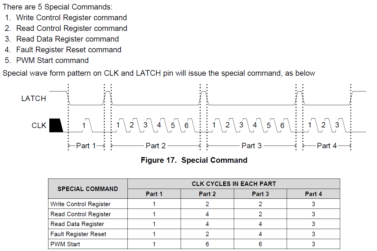
1. The beginning and end of the timing sequence in MSP430 reference routine are different from those in the data manual. For example, the last latch should be low level, and the statement of routine is commented.

2. Read the fault register data in strict accordance with the time sequence of the data manual, and found that the highest and lowest bit of data are incorrect, so refer to MSP430 routine to modify the program.

3. Now it is found that the first reading of fault register data is correct. Once the reset fault register operation is executed, the data read immediately after fault register reading is wrong, which is similar to moving one bit to the left, that is, the highest bit and the lowest bit error. So I added "CLK" to the beginning of the sequence_ H”“CLK_ In this way, it is correct and correct, but we can't find the basis and I don't know whether it is feasible.

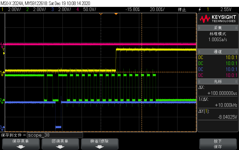
4. The figure below is the test waveform according to the routine. All 8 out are open circuit, the data read theoretically should be 0x00ff, and the measured data is correct for the first time. After the fault register is reset, the data read again is 0x01de

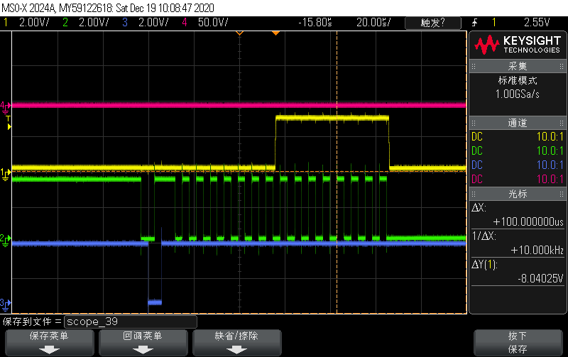
5. The figure below shows the test waveform of adding an extra clock pulse before reading the fault register timing according to the routine. All 8 out are open circuit. The data read in theory should be 0x00ff. The measured data is correct for the first time. After resetting the fault register, read the data 0x00ff again, which is still correct. Continue to try to restore the normal connection of different out interfaces and open circuit and short circuit test, and the reading is correct.

Blue is dout, green is latch, and yellow is CLK

The following is the procedure of this part, please see if it is feasible.

uint16 DRV8860_ReadFault()
{
uint16 dat=0;
uint8 i;

CLK_H();//
CLK_L();//

CLK_H();
LATCH_H();
CLK_L();
LATCH_L();
CLK_H();
LATCH_H();


for (i = 0; i < 8; i++)
{
CLK_H();
CLK_L();
dat <<= 1;
if (DOUT_PIN) dat |= 1;
}

for (i = 0; i < 8; i++)
{
CLK_H();
CLK_L();
dat <<= 1;
if (DOUT_PIN) dat |= 1;
}
DRV8860_Delay();
//LATCH_L();
return dat;
}

while(1)
{
drv8860.stu_fault = DRV8860_ReadFault();
b_8860_Hot = (drv8860.stu_fault) ? 0 : 1;
if (!b_8860_Hot)
{
DRV8860_RESET_FAULT_CMD();
}
Delay_ms(10);
}

  • Yunlong,

    I cannot see the waveform. Would you compare the good read command and bad command's CLK, nSCS, SDI, SDO scope waveform?

  • The following are the waveforms that the fault register can read correctly and the waveforms that can not be read correctly under the two test conditions of drv8860. The first two waveforms are all open circuit conditions for 8 out, and only the fault register is read. The last two are the conditions of out1 open circuit and out8 over-current. The program circulates to read the fault register, then clear the fault register, and then write to the data register 0x00. The only difference between right and wrong is that the program that reads the fault register has an extra clock high and clock low at the beginning.

    1、The following is the correct test waveform (all 8 out remain open)

    The data read by the fault register is correct: 0b0000 0000 1111 1111.

    The function of reading fault register is:

    uint16 DRV8860_ReadFault()
    {
    uint16 dat=0;
    uint8 i;

    CLK_H();
    CLK_L();

    CLK_H();
    LATCH_H();
    CLK_L();
    LATCH_L();
    CLK_H();
    LATCH_H();

    for (i = 0; i < 8; i++)
    {
    CLK_H();
    CLK_L();
    dat <<= 1;
    if (DOUT_PIN) dat |= 1;
    }

    for (i = 0; i < 8; i++)
    {
    CLK_H();
    CLK_L();
    dat <<= 1;
    if (DOUT_PIN) dat |= 1;
    }
    DRV8860_Delay();
    //LATCH_L();  The reference program of MSP430 blocks this instruction and the manual is lowered
    return dat;
    }

    Yellow color:  DOUT

    Green color: CLK

    Blue color: LATCH

    Red color:  DIN

    2、The following is the wrong test waveform (all 8 out remain open)

    The data read by the fault register is Error: 0b0000 0000 1111 1110.

    The function of reading fault register is:

    uint16 DRV8860_ReadFault()
    {
    uint16 dat=0;
    uint8 i;

    //CLK_H();
    //CLK_L();

    CLK_H();
    LATCH_H();
    CLK_L();
    LATCH_L(); 
    CLK_H(); 
    LATCH_H();

    for (i = 0; i < 8; i++)
    {
    CLK_H();
    CLK_L();
    dat <<= 1;
    if (DOUT_PIN) dat |= 1;
    }

    for (i = 0; i < 8; i++)
    {
    CLK_H();
    CLK_L();
    dat <<= 1;
    if (DOUT_PIN) dat |= 1;
    }
    DRV8860_Delay();
    //LATCH_L();  The reference program of MSP430 blocks this instruction and the manual is lowered
    return dat;
    }

    3、Correct waveform of the second test condition (out1 open circuit, out8 over current)

    a.The procedure is similar with the first one.

    b.After reading the fault register, execute the clear fault register instruction, and then write 0x00 to the data register.

    c.The data read by the fault register is correct: 0b1000 0000 0000 0001.

    3、Error waveform of the second test condition (out1 open circuit, out8 over current)

    a.The procedure is similar with the Second one.

    b.After reading the fault register, execute the clear fault register instruction, and then write 0x00 to the data register

    c.The data read by the fault register is Error: 0b0000 0000 0000 0010.


  • Yunlong,

    I am on vacation this week. So, the response could be delayed.

    I just checked the datasheet: There are 5 Special Commands need a extra click signal (part 1 clock) in front of the latch pulse. Does it explain your case?

  • Hi,WangLi

    I understand the meaning of your reply, but it has nothing to do with the reading fault register question I consulted. Reading the fault register does not belong to 5 special instructions.

    I has questions about the beginning of the sequence of reading the fault register. If I writes the program according to the manual sequence,  will lose the highest bit when reading the data. If it is configured as follows, it can be read correctly.

    Question 1:The beginning and end of the timing of reading the fault register in the reference program of the MSP430 evaluation board are different from the data sheet。Assuming that the MSP430 reference program is correct, I found that the data of the fault register is shifted to the left in the first reading, and the highest bit will be lost. The second and subsequent readings are correct. If I add CLK high and CLK low, Then the reading is correct the first time and afterwards, but there is no reliable basis for this operation, I don't know whether it is feasible.

    Question 2: If I do not add CLK high and CLK low, the highest bit will also be lost.

    Question 3: CLK_H();//? According to the datasheet timing diagram, it should be after LATCH_H; it cannot be read correctly after replacement.

    uint16 DRV8860_ReadFault()

    {

    uint16 dat=0;

    uint8 i;

    CLK_H();//?According to the datasheet sequence diagram, no need

    CLK_L();//?According to the datasheet sequence diagram, no need

    CLK_H();

    LATCH_H();

    CLK_L();

    LATCH_L();

    CLK_H();//?According to the datasheet sequence diagram, it should be after LATCH_H;

    LATCH_H(); 

    //LATCH_H();//The following is consistent with the datasheet, missing MSB

    // CLK_L();

    // LATCH_L();

    // LATCH_H();

    / // CLK_H();

    for (i = 0; i < 8; i++)
    {
    CLK_H();
    CLK_L();
    dat <<= 1;
    if (DOUT_PIN) dat |= 1;
    }

    for (i = 0; i < 8; i++)
    {
    CLK_H();
    CLK_L();
    dat <<= 1;
    if (DOUT_PIN) dat |= 1;
    }

    LATCH_L();//
    return dat;

  • Hello,

    I understand the problem you are having, but don't know how to explain why the extra clock pulse is working.  Before LATCH pulses low, the clock signal should be a "don't care". 

    That additional clock pulse you added to fix the issue should have been completely ignored by the device as far as I can tell from the timing diagrams in the datasheet and only the first high-low transition on the clock should shift out a bit.  

    From your first post, I have underlined my concern:

    3. Now it is found that the first reading of fault register data is correct. Once the reset fault register operation is executed, the data read immediately after fault register reading is wrong, which is similar to moving one bit to the left, that is, the highest bit and the lowest bit error. So I added "CLK" to the beginning of the sequence_ H”“CLK_ In this way, it is correct and correct, but we can't find the basis and I don't know whether it is feasible.

    Is it possible that the "Fault Register Reset" command is somehow not being done correctly (special command sequence is copied above)?  Can you show the scope capture with the reset command being sent BEFORE you do the read?  

    Since the reads are correct after this first read, I am curious what is about the reset procedure that could be related to the issue you are having.

  • Hello,

    Thank you very much for your reply.I am sure that the special instruction to reset the fault register is correct. In addition, it may be that my expression is not clear. The error of first reading the fault register exists in both cases. First, the program is executed from main, the first reading is wrong, and the second consecutive reading is correct. Second, as long as the fault register is reset, the first reading is wrong, and the second consecutive reading is correct.The middle section of the test waveform of this problem has the waveform of resetting the fault register.

    Below, I will attach a separate reset operation waveform.

    Yellow color:  DOUT

    Green color: CLK

    Blue color: LATCH

    Red color:  DIN

  • Hello again,

    It appears there was another customer with this issue and just found the post on it.  Please scroll to the last response before this was closed.

    It looks like this extra clock cycle is required to avoid the issue you are seeing.  Unfortunately, it is not documented in the datasheet, but proven to correct the issue.

  • Hi,Ryan Kehr

    I am very glad to see your reply. Can you arrange someone to test it? Verify the problem and solution I described.

  • Did you look at the post from Rick that I tagged above?  Rick did test it.  Problem and solution were verified.