This thread has been locked.

If you have a related question, please click the "Ask a related question" button in the top right corner. The newly created question will be automatically linked to this question.

DRV8353: Problems with newer Batch NR. TI98F TI99F

Part Number: DRV8353

Hello,

*********DRV8353RSRGZ*********

Last Year, we designed our own power electronics with the MOSFET Driver DRV8353RSRGZ. In the beginning we had a lot of Problems with destroyed DRV's, because of bad designs of our Power Stage and bad Settings of Gate Drive Current. We tried 5 Different designs of Prototypes to get a solution that works. 

The design has been in use since the beginning of 2020 is verified to a phase Current of 350A and is nearly one year tested in a small series of 20 Controllers.

The Batch No. of the Parts in the small series is TI88F. 

Actually we produced new Boards of the verified and tested Design, with newer DRV's (Batch No. TI98 & No. TI99). 

We have the Problem that the Mosfet Driver with the higher Batch No. (TI 98 & TI99) dies at 140A Phase Current. We tested this time 8 Boards with DRV's from this Batch No. and on every Board dies the DRV quickly. At 140A phase current, the driver on the low side is destroyed at random phase.

To check whether it is a design or a component failure, we soldered DRV8353RS's from a previous order (Batch No. TI 88F) onto exactly these boards. With the "old" DRV (TI88F) no problems could be found and the function up to 350A phase current could be verified on exactly these boards. 


We got the Driver (TI98F und TI99F) from different Distributors, so a delivery damage is not impossilbe.
The parts (Batch No. TI98F) are from Mouser and the Parts (Batch No TI 99F) are from TI directly. 

Are there any Changes or is there any Product Change Notification we can't found, between the BatchNo. TI88F - and TI98F /TI99F?


We have a real headache to use this parts in a serial Aplication

Thank you in advance,

Jörn

  • Hello Jörn,

    I agree with most of the assessment, its very unlikely to be shipped damaged parts.

    These types of situations are actually very difficult but we can get the process started.

    Wafer Process Variance

    These requests are not easy to fulfill in a generic sense. The type of info we need to fulfill that request is to understand what specific FET was damaged within the design and take a look at that model specifically and do some cross referencing. Without xray, decapsulation, and images of the damage site, we cannot say with any confidence what drifted between the wafers. To reiterate, while the datasheet might only show a pull up and pull down FET in the gate drive circuit, in reality, there are hundreds (for example, each IDRIVE setting is a cascaded FET with a different W/L ratio to provide a different I_D that matches with the setting), all with different functions and specifications that can be tracked and can vary.

    So, I would prefer to shelve that question for now as I have some other comments and questions first.

    Walking wounded vs. catastrophic damage:

    It sounds like the design stage has not been easy. Though it sounds like you've got a working prototype, with a specific wafer lot trace code, it sounds like you weren't far enough in the validation process to see if it passed any "stress over lifetime" type tests (though a year is a long time, but 20 is not a large sample size). Please correct me if I'm wrong.

    This means, we can't be certain if the process variance holds the key to a successful product. We've seen that parts that fail earlier in the design phase will indicate that the system is not robust as process variance may postpone the damage till much later in the system's lifetime. Does this make sense? Essentially we can't determine if the first batch was "wounded", or working but will fail before its expected lifetime, compared to the second batch which "died" relatively quickly within its lifetime.

    These are the reasons why I want to pivot the discussion and instead understand how to make your system more robust. From our (TI's) perspective, we provided the process and temperature variance through the min and max electrical characteristics specifications in the datasheet. So, if there's a gap in our datasheet, we want to know that. If we missed something in the design, we also want to know that. Right now, we have no idea what kind of root causes could be associated with this result.

    More robust design:

    If you knew the root causes of damage leading up to the working solution you had with the first batch of devices, then we should be able to compare that against the damage you have now and see if they match. It sounds like you haven't done that analysis yet, and I hope you did that analysis beforehand. The classic one for this device is seeing VGLS or the GLx pins suffering damage, so I recommend a quick impedance test there. Waveform comparisons between good and bad devices help too.

    You've already mentioned gate drive current and power stage "design", though I don't see any E2E posts from you in the pasts. We have plenty of tips: gate resistors, snubbers, C_GD caps, diodes on gates, complete layout recommendations, and others. So we can help in any way we can.

    As such, let's figure out possible root causes, and we can propose some possible solutions or workarounds, which could give us some hints for the actual root cause where we can leverage the lot trace codes as evidence, not as the solution.

    Let me know what you think.

    Best,

    -Cole

  • Hey Cole,


    thank you for your interest :)


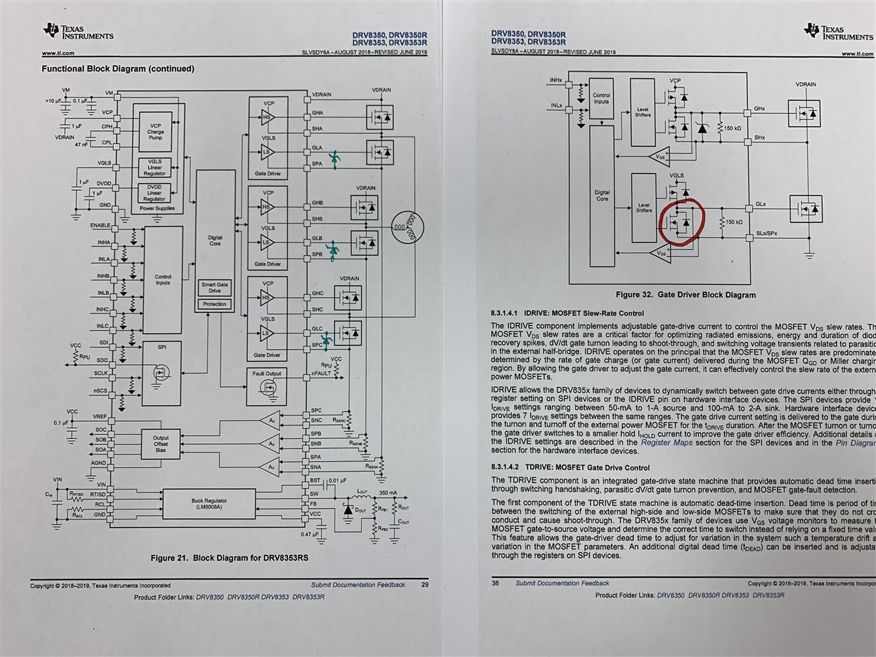
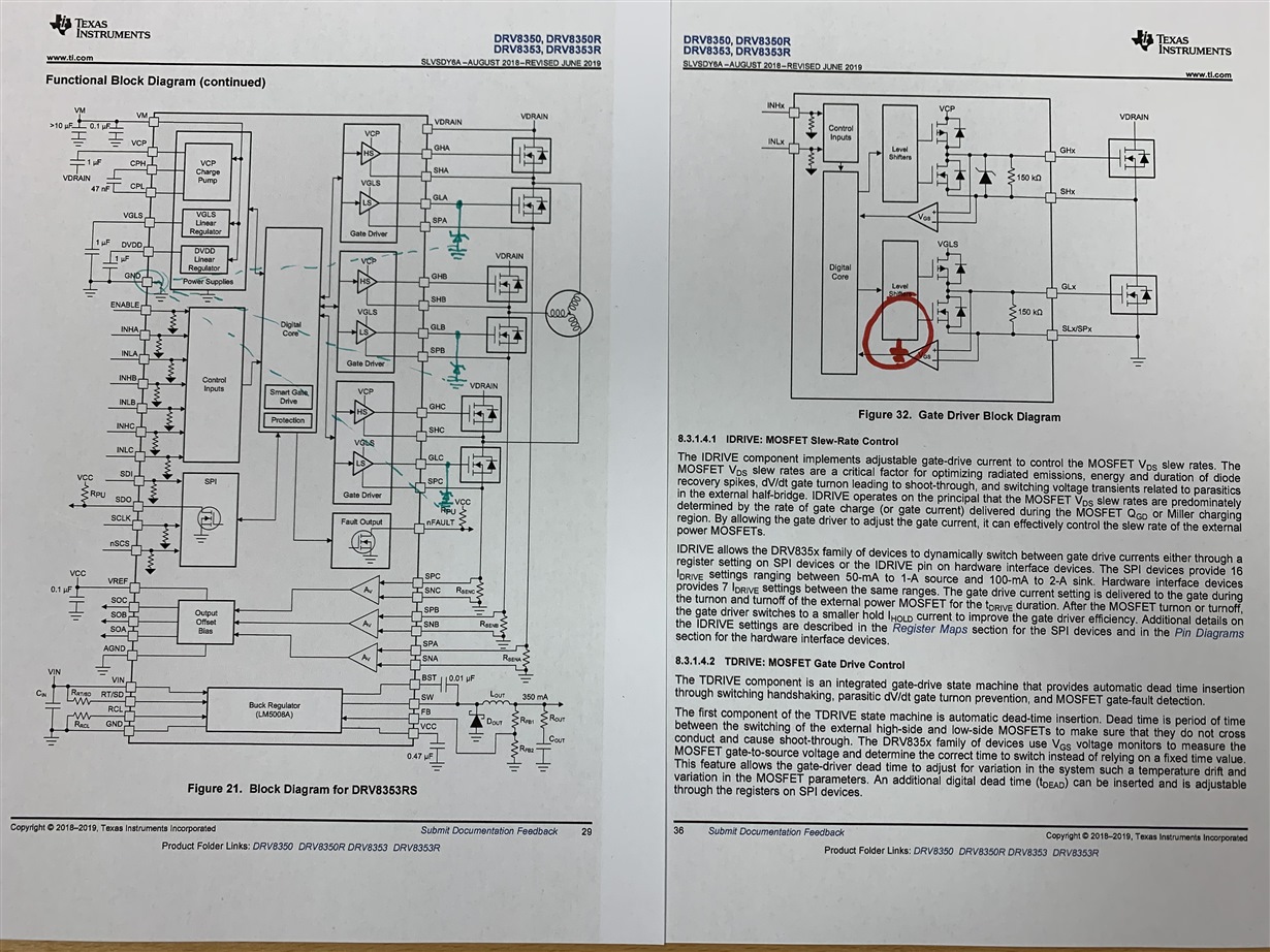
    i told you that the low side Driver dies directly at (for us) low Phase Currents of 120A. For a little failure analysis, I removed the damaged part from the Board and measured the resistance of the GLx Pin to VGLS, GLx to GND and VGLS to GND. Which low side dies is randomly. Sometimes A and sometimes B


    Glx to VGLS       142Ohm
    Glx to GND         893kOhm
    VGLS to GND     893kOhm


    The Fault Registers show a GDF and VGLS UV Fault. The latched GDF can be cleared, but the VGLS Fault remains.

    If I solder an older DRV ( TI 88F / TI89F) on exactly these Board the system works great. :(

    To understand our Case und what we have done, I want to give you a short summary of our Board and our development. Maybe you see something we did wrong or you can give use some advices for a more robust design.


    Requirement profile:

     70V
    250A Phase
    100A Battery
    FOC with Hall Sensors

    In the first prototypes we start with the topology of 3 parallel Fets per Phase with Snubbers, Gate Source Caps and different Idrive Settings. At first we didn’t have much success with this system, we had Problems with dieing Fets. The Reason was, that we drove the FETs without Gate Resistors, so they doesn’t switch exactly at the same time and one Fet was more stressed then the other.
    We added Gate Resistors for every single Fet, to balance the drive Current between the FETs. The result was much better, but not good enough.
    At Higher Currents (180A), we got a permanent VLGS Fault.
    We analyzed that problem and find out, that in case of hard switching a peak on the Gx Pin occur. The Peak occurs when Vgs reaches the Mosfet threshold and the FET gets conductive, in this moment the Body Diode of the High side FET must be deload and it comes to a short shot-through. The Shot-through takes care of the Peak between Gx and GND Pin of the DRV. Is the Peak Higher as the 18V VGLS / GLx maximum Ratings, the DRV is dieing.

    Channel 1 GLx; Channel 2 Phase Voltage 


    In summary we had to reduce the Trace between the DRV and Low side source, to decrease the peak in the Hard switching moment and we changed the topology of the FETs to one single FET for each switching point, then we could dispense with Gate resistors and can control the switching behavior by Idrive Settings.

    We customize our design and were very success in the first test’s… We could drive phase currents up to 300A and had since the beginning no problems with dieing DRV’s

    We actually use the Driver with the following settings:
                  
    Reg 0x02: 00000000 00000000 (0x0000)

    Reg 0x03: 00000011 01101001 (0x0369)  //   Highside Idrivep 400mA; Idriven 1200mA)

    Reg 0x04: 00000111 01011001 (0x0759)  //   Lowside Idrivep 350mA; Idriven 1200mA / Tdrive 400ns

    Reg 0x05: 00000001 01011010 (0x015a)

    Reg 0x06: 00000010 01000000 (0x0240)

    Reg 0x07: 00000000 00000000 (0x0000)


    Our Board Details:

    6Layer 70um Copper
    No Gate resistor, no GD caps
    Snubber at High and Low Side (1Ohm 10nF)
    Highside Idrivep 400mA; Idriven 1200mA)
    Lowside Idrivep 350mA; Idriven 1200mA / Tdrive 400ns
    single Mosfet topology --> Mosfet  FDBL86361-F085 (Qgd 34nC ; QGs 51nC)

    I would prefer to send you pictures of the design private, therefore I did a friendship request :)

    best :)

     Jörm

  • I did some Tests with the newer Batch No. Ti 98

    The Peak on the GLx Pin at the Hard switching event is not more than 12V, when the DRV is dieing.
    I don't think that is the reason of the problem.   

    I also tried lower IdriveP (down to 150mA) on the low Side, this makes also no difference.

  • Hello Jörm,

    Summary comments

    Thanks for the info. Shoot through in the previous prototype is definitely different than what we're experiencing here.

    Knowing its a VGLS to GLx  short helps a lot. Random phases receiving the damage means that layout of the phases are equally considered (or if there is a clear offset, where one phase is clearly worse in layout, it means layout of the gate drive traces has a decreased role in the problem). Anyways, I'll accept the friend request and take a look after our next steps here.

    Next steps

    Can you clarify the tests a bit? Am I correct to assume that the lower IdriveP (150mA) still caused damage to the device and the voltage spikes seen during this use case were no more than 12V? Have you tried IdriveN to a lower value.

    Lowering the IDRIVE is usually the number 1 workaround that will make any spikes smaller and any possibility of damage, disappear. As a general note, I do think 1.2A is far too much for the Q_GD of those FETs, I would do no more than 300mA for IdriveN (fall time) and 350mA for IdriveP (rise time) for the purposes of this debug.

    The next step I would do is monitor VGLS waveform (the probing of GND near the VGLS cap GND and GND pin are very important to check if ground is bouncing around. This would mean the negative waveform is causing GND to bounce near the FETs which leads to difference in potential as current goes into the VGLS pin as the INLx pin turns on and tries to source that current. This is different from the previous theory as the source of energy comes from the VGLS pin instead of the GLx pin.

    Again, lowering the IdriveN will reduce negative bouncing for the GND net and I would expect the problem to reduce or go away entirely. If you want to try and monitor this, the GND probe lead location is extremely important to get good data. Differential probe even better. GND pins vs FET lowside sources vs. VGLS cap GND should also see different levels of voltage because of the parasitics. But again, lower IdriveN first and see if the problem goes away, and if it doesn't, we can start probing.

    Best,

    -Cole

  • Hi Cole, 

    yes i also think that the gate drive traces are not the root cause of the problem, 
    i already thought about that 1.2A are to much sink current, but we had no problems with this setting before :/ ... this will be the first thing i will try and give a report. 

    did you forget the request? i can't send you the design files 

    best :)

  • Hello Jörm,

    For your info, the source gate drive current control rise time and sink gate drive current control fall time of the gate signal. Because the parasitics don't change in the system, and we saw reducing rise time was able to improve performance, I expect reducing fall time will also do the same. I will say, usually the fall time effects seem to affect the system less because users will usually put precedence over GND layout instead of VDRAIN and SHx layout, which means negative transients affect the system less.

    You can check out the theory behind this logic in the E2E post for more info: 


    Also, yes, I should have accepted the request now.

    Best,

    -Cole

  • So, i send you the design files private.

    today i tested the lower i drive Setting 

    Reg 0x03 --> 0x0363  --> Highside IdriveP  400mA IdriveN 150mA
    Reg 0x04 --> 0x0743 --> Lowside IdriveP 300mA IdriveN 150mA

    The result was a bit better. The controler was able to do a phase current of 170A (before 140A) until the driver dies.
    Same Fault-profile as before GDF Low A  and VGLS UV.

    i have some (not very detailed) scope pictures, last triggered before dieing (170A) . 

    probe points are:
    GND both channels --> VGLS Cap GND
    red Channel    --> Low A Gate (0 Ohm Gate resitor directly on the DRV)
    blue Channel  -->  Low A Gate (directly Mosfet)

    last one (picture 32 of 32)

    (picture 6 of 32)

     picture 7 of 32


    what do you think about the result and the scopes?  
    And what would you suggest for the next steps?
    And how can it be that older DRV's are not so delicate? 

    best 
    Jörn

  • Hello Jörn,

    Thanks for the waveforms. I actually think this is the same symptom as you mentioned before. When I think of ripple caused by gate drive current, I expect the ripple and overshoot to occur at the end of the transition from high to low or low to high. The voltage spikes here are happening either a short time after or during the transition. I would suspect that another gate is turning within the same half bridge phase which is causing the spikes. Instead of shoot through, this is the 

    The absolute max spec for GLx at 200ns transient are -5V, and we're not zoomed in enough to see if this would violate the spec but I suspect the spike increases as current through the half bridge increases (which leads to a higher spike and the damage we see).

    As such, I suggest you increase DEAD_TIME (0x05[9:8]) to 400ns or 200ns (0b11 or 0b10) and see if the spike disappears. If not continue to lower the gate drive current on both even further (and if you hit the minimum, maybe even replace the 0ohm gate resistors with 3-15ohms).

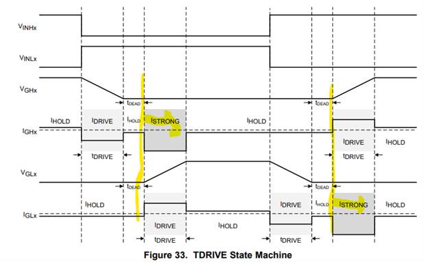
    My current hypothesis is that the spike in picture 6 is much lower because we were able to hit the ISTRONG section of the state machine which was able to pull more current out of the gate prevent the gate voltage from spiking. This is contrasted with picture 32 where the gate transition and spike happen towards the middle of the dead time, which means the gate is starting to turn on, relatively, much before the state machine could transition to ISTRONG  

    The dead time just gives the state machine more time to attempt to get into the ISTRONG section and lowering the gate drive current causes that ramp of the voltage to go slower, so the "almost shoot through" transconductance event will happen at a lot slower rate and hopefully give enough time for ISTRONG to occur, which would also lower the spike.

    I would assume this is because TI88 and TI9x have had a silicon shift in the timing specs. We don't specify the dead time specs with a min and max, only a typical. My rough analysis shows it can vary 50% to 200% depending on the process node. Looks like TI9x shifted in the "shorter or <100% of typical spec" direction compared to the TI88. 

    Anyways, this is my guess. Feel free to try the suggests and see if the spikes reduce. And if they don't try to capture the GHx at the same time and see if we can cross reference those spikes with another gate signal.

    Best,

    -Cole

  • Tank you Cole,

    We tried a lot in the last few days. We varied the dead time and found that the spike also migrated. After that we reduced the idrive Settings to IdriveP 350mA and IdriveN 300mA at Low and High side. For comparable measurements and tests, I let the motor run with 100A phase current and 10% duty cycle

    ***( blue --> GLA, red --> phase) *** reference signal with short dead time ****

    Based on these waveforms, we assumed that the negative spike would destroy the driver.
    To reduce the negative spike, we placed diodes (TS4148RYG; Reverse recovery time 4ns) from GLx to GND (VGLS Cap)
    The result is better, the driver is still working even with higher currents too. 


    ***negative spike with diodes *** blue --> GLA ; red--> phase ****

    There are still a few questions left. 

    1. Is it the right way, to place diodes from GND(VLGS cap)  to GLx? 

    The datasheet shows two cases, drive from GND and drive from SP/SLx?

    which one ist the right way? a) or b)?

    2. The phase voltage overshoot at the end of the transition from high to low or low to high. 

    *** blue--> GLA ; red--> phase ***

    How can we prevent this event? i think the Idrive Settings are low enough? Also also think the fall time of Gate voltage is very slow, what is your opinion?

    3.  At these overshoots we have a spike between SPx and SNx 
    We have Shunt resistors of 0,0005 Ohms.

    ***red-->phase; blue--> Shunt voltage; black--> calculated current***

    i think this is related to question 1.


    The Gate Driver is still working now, but I think the wave forms are not optimal, how can we optimize them?

    best :)

  • Hey Jörn,

    Happy to hear about the results, I agree there's some more work to be done. Note, your first "no C_GS cap" didn't load properly. I assume its a similar picture,  but the spikes are larger compared to the C_GS cap case.

    1. Is it the right way, to place diodes from GND(VLGS cap)  to GLx? a) or b)? Also, The datasheet shows two cases?

    Assuming the purpose of the diodes is to suppress transients on the gate during very high voltage events, I would recommend a), as the goal is to divert energy away from the pin, which would case damage. It may cause a bounce but this kind of transient protection is supposed to be during extreme cases where the driver needs to start braking or shutting down safely (which is usually once in a while kind of operation) and not every PWM.

    Trying to prevent spiking every PWM can be done other ways, more on that later. But we can open up the discussion further, if you want.

    Also, the difference between the two diagrams is one is emphasizing the V_GS monitor locations and one is emphasizing the V_DS monitor locations so both are correct (but neither show the shunt or sense resistor, which is present in your design).

    2. The phase voltage overshoot at the end of the transition from high to low or low to high. Gate voltage is very slow. 3.  At these overshoots we have a spike between SPx and SNx

    Its pretty clear what's happening now, thanks for the waveforms (though the corresponding GHx waveforms would made it more comprehensive). 

    So what we're looking at, for 2, is as the FET turns off, the BEMF starts to become present again as VGS approaches Vth to turn off. Then as the FET channel collapses and we reach the top of the voltage square wave on the phase. The LC parasitics start the ringing in the waveforms even though the gate voltage isn't completely off yet. 

    I also agree >400ns is a very long time to turn on and off the gate.

    As such, I think we're going to need VDRAIN to SNx capacitors for each leg to help with the negative spike. Decoupling capacitance from VDRAIN to GND will help with the positive spike. Some might introduce an electrolytic for the bulk cap VDRAIN to GND at this point or a big bulk bank of ceramics but extra care must be taken to reduce parasitics between the farthest bulk cap and the drain of the HS FET.

    To speak generally, I'm not sure how much decoupling capacitance you have but thermal connections for components add inductance in the line which decreases effective capacitance the father the capacitor is from the drain of the FET. Note, thermal connections are when the pads look spoked instead of direct connections where copper completely surrounds the pad. See thermal connection section 2.4 of the layout app note for a visualization: https://www.ti.com/lit/an/slva959a/slva959a.pdf 

    You could also look into adding RC snubber on each leg but these usually reduce ringing and settling time, not so much overshoot. So if you add in capacitors and try to increase the gate drive current again, you might see a smaller overshoot but ringing might be for a longer duration; which is where the RC snubbers come. The phase looks pretty flat after the one overshoot so you might be able to do without it. I'll leave this blog about snubber design just in case: Power Tips: Calculate an R-C snubber in seven steps

    Note that you want to try some of these on your existing board, floating wire used to add components might introduce series inductance which might not help mitigate the effects. So just be ready. If you see better performance, its an indication it'll only get better with soldered down components and footprints.

    Let me know what you think.

    Best,

    -Cole

  • thanks,

    "Assuming the purpose of the diodes is to suppress transients on the gate during very high voltage events, I would recommend a), as the goal is to divert energy away from the pin, which would case damage."


    We want to use the Diodes to get safety, if a negative spike occurs and the Driver doesn't die. As i said, the system has been working fine for a year with these older DRV. You're right there is a negative spike and it is probably the reason why the newer ones dies, so in my mind the spike must be prevent.


    But the question is, what damage occurs in the driver? i think there are 2 cases.

    case 1:

    there is a damage(red) in the low side Fet of the driver... then i think diodes(blue)  from SPx to GLx will help

    or

    case 2

    there is a damage (red) in the level Shift... then diodes (blue) from GND to GLx will help.

    what do you think what damage occurs?

    Obviously are the Diodes the difference between the dieing DRV (Bach No. 9x) and working DRV(Batch Nor 8x).

    best
    Jörn

  • Hello Jörn,

    I owe you a more thorough answer for where we should put the diodes later. I'm hoping for on Friday 1/8/21 you can expect an answer.

    As for the source of the damage, again, I'll need to talk with the team. But in order to do this, you'll need to answer my private message I've sent to you.

    Thanks,

    -Cole

  • Hello Jörn,

    I'm going to close the thread here as the rest should be covered over email.

    Best,

    -Cole