This thread has been locked.

If you have a related question, please click the "Ask a related question" button in the top right corner. The newly created question will be automatically linked to this question.

DRV8323: multiple issues with DRV8323H, nFault Pulsing, Amplifier Output not working ...

Part Number: DRV8323
Other Parts Discussed in Thread: DRV8302, , DRV832X

Hi all, 

We just recently made a new design with intention of migrating from legendary DRV8302 to DRV8323H ( No SPI) and up to now we are having, unfortunately, a very bad time with it ( maybe too much smart gate driver is not good in analog and power electronics ...)

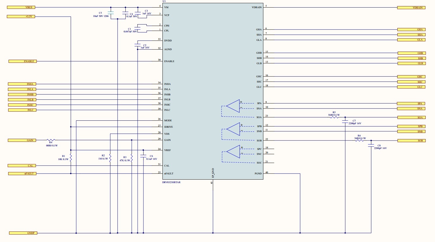
anyways, below I will share firstly our schematics of DRV and the MOSFETs:

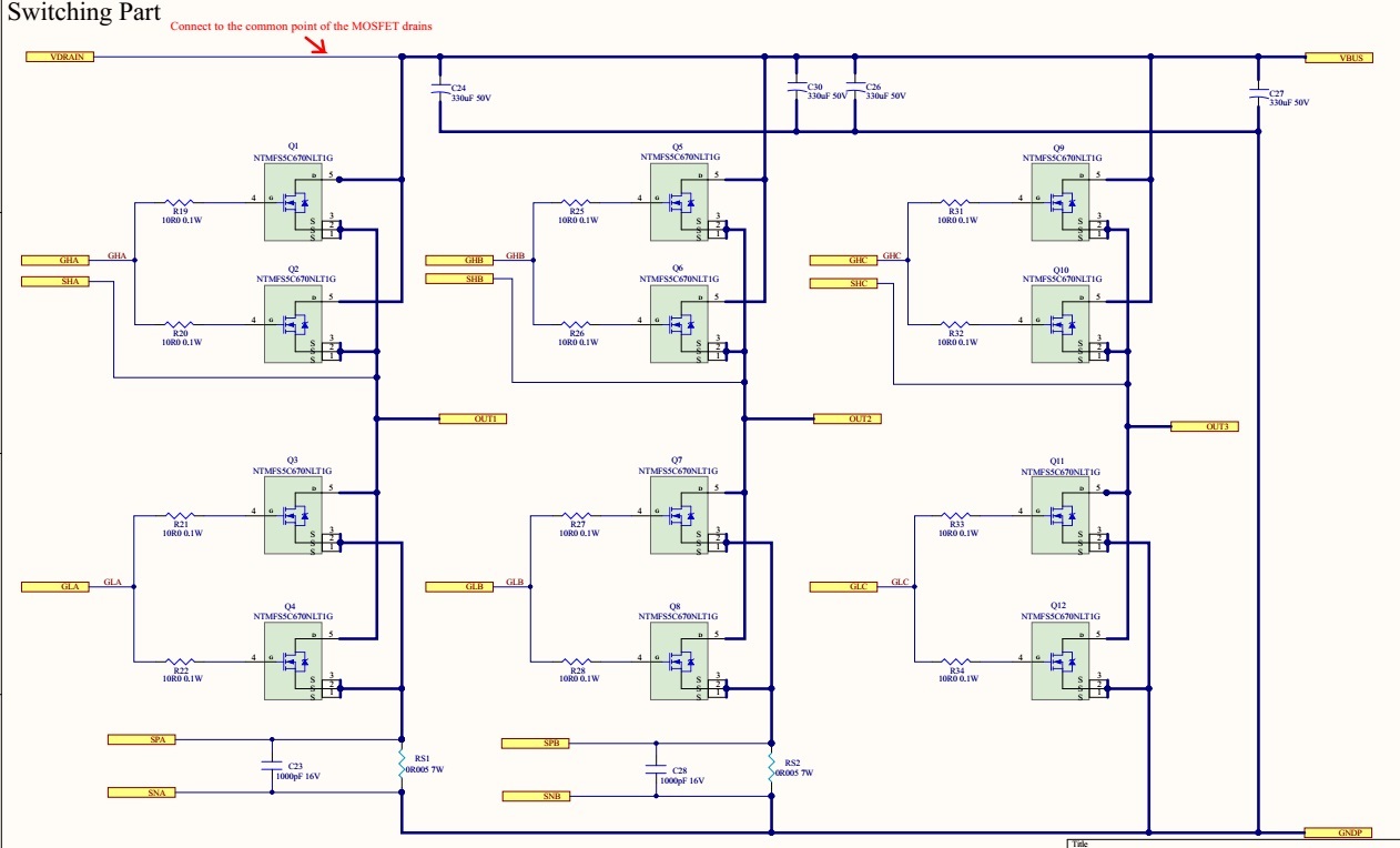
as you can see, we are using parallel MOSFETs for multiple reasons and this is our preferred way of proceeding as we did this before with no issues with DRV8302. All the gate paths to DRV IC are having an equal length and we think the layout design is good enough.

We are using two shunts and the third channel of DRV8323 is unused, and we didn't ground the inputs of that, can this be an issue?

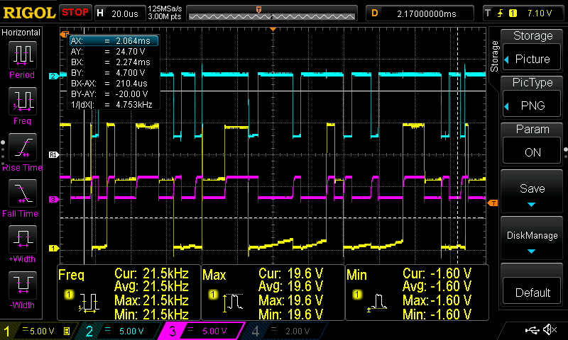
- Once we turn on the device, and apply PWM inputs to the DRV, we see that the nFault pin starts to pulse as below, while we see the switching at the output, but of course due to fault, the Motor is jogging and not moving... ( the same algorithm on DRV8302 works flawlessly). The switching freq. now is 20kHz.

it's almost impossible to understand what this fault means, I think the chip design team, could define different timings for different errors on fault pin, so it was at least possible to understand what type of error we are receiving in hardware mode design.


++ The second issue is, we don't see any output at the Amplifiers outputs, just a noisy signal around the 1.65V. to verify that, we tried to turn the motor manually and see if there is any current detected from that output, we saw no difference. ( The CAL pin is kept low )

We also tried to replace the chip after multiple tests, but no difference.

pls let us know where are we going wrong?

Regards

  • The images are missing from above are :

    Switching part:

    nFault situation:

  • Hello John,

    nFAULT problem:

    I think we can learn quite a bit from you waveform in regards to the fault. Looks like there's a bit of periodicity to the signal. It is in the time frame of 5us pulse width and, at fastest, 200kHz. This is faster than your PWM switching frequency and the nFAULT doesn't latch so this rules out overcurrents, thermal shutdown, gate drive faults, and VM UVLO which just leaves VCP UVLO (and maybe VGLS problems, but we'll get to that).

    As a result, can you please measure VCP, with good probing techniques so that the GND lead of the oscilloscope probe is at the GND pin, V_GHx, V_GLx, and nFAULT on the same waveforms and see if anything lines up? If VCP doesn't seem to be the problem can you keep V_GLx low and try to switch V_GHx and see if nFAULT toggles and then repeat the process by keeping V_GHx low and V_GLx toggled?

    So far, I don't see anything wrong with the schematic.

    CSA

    Also, keeping the inputs to the unused CSA is not recommended, as floating inputs mean the output could toggle for no reason and introduce noise into the system, but its unlikely. It definitely won't interfere with the nFAULT and gate drive problem. Its best to at least tie the inputs together and to a known voltage if possible.

    Spinning the rotor to generate BEMF doesn't generate current if the none of the gates are on to allow current to flow to through the lowside FETs and into the sense resistor. Because your VREF = 3.3V, I would expect the Vo = 1.65V or 3.3/2, as SPx - SNx = 0V in the situation you've described.

    As such, I would just remove the motor and force known voltage at SPx with a source meter so you can compare the output against the equation in the datasheet. 

    Best,

    -Cole

    Edit: If you haven't adjust the gate drive current from the maximum and sized it according to the Q_GD of your FET, you might have damaged the part. See post here:  

  • Thanks, Cole for the answers, 

    Yeah, I approve that the VCP is stable and according to specs, so the problem is not there, however, I have monitored GLA, GHA, and the nFAULT pin against Ground as below:

    Blue: GLA
    Yellow: GHA
    Purple: nFAULT ( Low : Error, High: Normal)

    The waveforms of GHA and GLA seems strange to me, so I have some opinions because the same exact inputs to DRV8302 which is on 6X pwm Mode generates propper switchings, but here it seems the pattern is not right...

    so my guess goes for Mode selection on DRV8323H, as you can see, we have selected the 6x PWM Mode by connecting Mode pin to Ground, but in DRV8302, we have selected the 6x PWM mode ( independent). so maybe this is the reason that the switching pattern doesn't match??

    Thanks in advance.

  • Hello John,

    I know the datasheet for the DRV8302 says "independent" 6x PWM mode but if you look at the truth table the INHx = 1 and INLx = 1 case still equals GHx=0 and GLx=0 which matches the DRV832x 6x PWM mode. For independent mode INHx = 1 and INLx = 1 would equal GHx=1 and GLx=1, which could result in shoot through in a half bridge configuration.

    Edit: talked with the team and made some assumptions to ignore crossed out text:

    As for the fault, I'm going to guess you are hitting an OCP of some sort, could be VDS_OCP or could SEN_OCP. We know this because a new PWM signal will clear the fault when the CBC or cycle by cycle current limit is enabled (which it is by default for hardware devices); which is what we see here. So, you might want to increase the setting on the VDS pin and see if the problem goes away. If you had a current probe, this might be easier to verify as you could see what current is flowing through the motor phase and correspond that with the VDS level you have.

    Best,

    -Cole

    As for the waveform, I'm not sure what to make of it as it looks very very incorrect for a lot of reasons. If you can capture the corresponding INHx with GHx, nFAULT, and SHx it'll be more helpful. Then another waveform with INLx with GLx, nFAULT, and SPx. These would be helpful.

    You can see GHx trying to recover and pump up the voltage (like the charge pump) when the gate was pulled down, and you can see a VM/2 on GHx like the BEMF is being fed back when the drivers are disabled as a result of the fault. And GLx is shooting maybe -10V in some cases? Which is outside of the abs. max for the pin, which could result in damage. So the part is already damaged or some regulator is dropping out and causing some weird behavior.

    I'm going to talk with the team about it and see if we can come up with. Otherwise, you can try replacing the part, sizing your IDRIVE correct in the blog post above and seeing if the problem goes away.

  • Hi Cole, Thanks for the answers, 

    Ok, I'm sorry, I forgot to mention that:

    1-The tests above have been done without the Motor being connected at the output, so the switching is done without any current going through the Motor, so the Overcurrent at least for the SEN_OCP probably is out of the equation.

    2- The BUS voltage intentionally left around 10V

    Now let's look again at the waveform, as you can see, from the Blue plot, which is the GLA, DRV8323 is unable to turn ON the low-side MOSFETs at all, there is always a "Strong Gate Pulldown" mentioned in SLVA714C and then afterward keeping the low-side MOSFETs always OFF. based on the mentioned article, this phenomenon occurs as mentioned : 

    "To protect against this scenario, the TDRIVE state machine of the Smart Gate Driver enables a strong gate pulldown on the low-side MOSFET while the high side MOSFET is slewing (Figure 14). The pulldown provides a path for the charge that couples into the MOSFET gate. " mentioned on Pg. 13

    it seems to me this is the problem...

    maybe due to the fact that the high-side Mosfets are turning On with very high dv/dt, due to very high IDRIVE and this causes the issue, but the amazing thing is that I've put even 2X to 3X more resistance on the path of Gate ( R_gate ) to see if anything changes and still the same behavior, I expect by adding resistance on the Gate's path, the IDRIVE will be forced to be limited!

    In the current test you are seeing, the GATEs of MOSFETs don't have any resistance, and they are directly connected to DRV8323 with 0-ohm GATE resistance...

    The switching pattern of the Mosfets is exactly identical to a product with DRV8302, and working flawlessly, so I don't see why the input signals can cause this issue....

    I will try to reduce the IDRIVE, but as you see, in our design, IDRIVE is connected directly to DVDD, and at the PCB level, so I have to cut through the PCB wires and hopefully being able to alter it, so if you and your team think the IDRIVE value is the cause of this issue, I'll proceed to apply the surgery on the PCB.

    Thanks in advance

  • Hi John,

    FYI - SPC and SNC should both be grounded when unused, otherwise the driver will throw a sense amp overcurrent fault.

    Thanks,

    Matt

  • Hello John,

    1-The tests above 

    Thanks for letting us know that no motor is connected in this test. The OCP is still voltage based so I don't want to rule it out just yet.

    2-unable to turn ON the low-side MOSFETs

    This is the most concerning part to me. If INLx is asserted and INHx is not, then GLx is supposed to be VGLS, this according to the table we've already taken a look at. I assumed that your waveform was offset, are you saying GLx in the signal is going from 0V to -10V? Its impossible for the DRV to apply negative voltage.

    Please keep the FW from the controller in an idle state and apply 0V to INHA and >1.5V to INLA and see if the GLA and SNA have the criteria to turn the FET on.

    The DRV is acting so weird that we need to verify some assumptions. Might even need to do a schematic review.

    Strong Gate Pulldown  seems to me this is the problem.

    The ISTRONG only occurs when the FET in the same leg is trying to turn on and nFAULT is not triggered. I don't see how this criteria is met from your waveforms.

    A fault condition will specifically float the gate driver output pins (with a very weak pull down to keep the source and gate tied together on both HS and LS). So I can't necessarily predict what the exact voltage on any of the pins will be when nFAULT is exerted.

    I'll proceed to apply the surgery on the PCB

    Changing the gate resistor does the same thing as reducing the gate current so you only have to do that.

    And I do understand that the DRV8302 worked fine. We unfortunately, added in the smart gate drive architecture, and a whole new schematic and layout between the two designs. Right now, I haven't isolated which is the problem yet.

    Best,

    -Cole

  • Thanks Matt, 

    Indeed this could be potentially the issue, I whish the datasheet was more strict and specific on this! Yes, this thing is mentioned in Pg 41 saying: 

    "If any of the three current sense amplifiers are not being used, they can be tied off by shorting the SNx pin to the SPx pin and leaving the SOx pin unconnected. Remember to connect the SPx or SNx pin to the low-side FET source, so that the overcurrent VDS monitor is still functional "

    to be honest, I don't get from this sentence the severity of not connecting the 3rd amplifier to the Ground of third leg half-bridge, it's not mentioning that FAULT will be exerted and it's kind of looking like recommending some sort of better design, may be it can be changed some how with stronger language and some warnings later in future ( the writers should consider who they are talking with, Mostly hardware engineers with very strict routines in design and readings :)) )

    by the way I will try to short some how SN3 and SP3 and see what will happen ( super hard, as I don't have access to those pins :(  )

    Thanks again 

  • Hi John,

    Yes, the datasheet wording needs to be stronger. This item about the sense amplifiers is on our list for the next revision of the DRV832x datasheet planned for the first half of 2021.

    Thanks,

    Matt

  • Hi Matt, 

    Today I found some time to apply the suggested edit on the PCB and I confirm that by connecting SPC and SNC to ground the nFault stopped being exerted and the DRV8323 now is working fine, I will continue my tests to see everything else is fine.

    Regards

    John

  • Hi John,

    This is very good to hear. Please keep us posted if you find any issues.

    Thanks,

    Matt

  • Hi Matt, 

    Yeah, So I could test the Motor spinning up to 30V, but after I raised the Bus voltage to 40V, The DRV8323 seems to get broken, so now, I want to refine my PCB design with much lower IDRIVE and grounding SPC and SNC in a new PCB to see finally how DRV8323 behaves. 

    I'm also going to Remove the GATE resistors, as Adam says here:

    "DON'T Use gate resistors unless they are required by your design. Gate resistors will complicate the IDRIVE setting and are usually not needed unless a safety or automotive requirement exists."

    As I understood before DRV8323 tries to keep the Mosfets' Gate ON, by controlling the current, and it seems adding a resistor will make the current control circuitry very complicated ( Keeping a constant current requires higher voltages and so on, correct me if I'm wrong pls), so it seems the idea of having GATE resistors is not a good idea in contrast to conventional GATE drivers ( Voltage based ones)

    I will continue to refine my design to reach a perfect point with DRV8323, I will keep you informed.

    Regards
    John

  • Hi John,

    You can leave the gate resistors as 0 ohm on the design as long as they don't add too much additional inductance in the path of the gates. If the gate resistor values are much smaller than 11V / IDRIVE, it is OK. We prefer to have the DRV8323 controlling the current rather than the external resistors.

    As you increase the voltage, the potential for ringing due to switching gets more likely, and you lose headroom to the 65V abs max rating of the DRV8323.

    If you are using 50V capacitors, bear in mind that they loose a significant portion of their value due to de-rating when operating at 40V. If you intend to operate at 40V DC, you may want to up some capacitor ratings to 63V or higher (i.e. CPH-CPL 47nF, VM 0.1uF).

    Do you know what pins were damaged on the DRV8323? We may be able to guess the cause.

    Thanks,

    Matt