This thread has been locked.

If you have a related question, please click the "Ask a related question" button in the top right corner. The newly created question will be automatically linked to this question.

TL5001A: TL5001A compensation network

Part Number: TL5001A
Other Parts Discussed in Thread: TL5001

Hello,

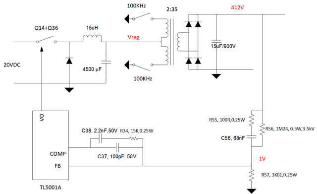
Old thread has been closed. I beg your pardon, but I have bought some new mosfets to replace IRF540N by IRFB4332 and UPS has lost my parcel !

With these new mosfets (that support 250V, 540N only support 100V), result is worse that with IRF540N.

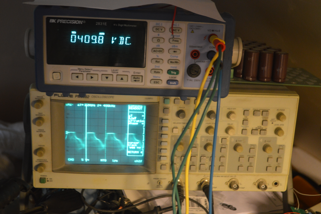
I have done a small video hilbert.systella.fr/.../2021-05-18-144931.webm

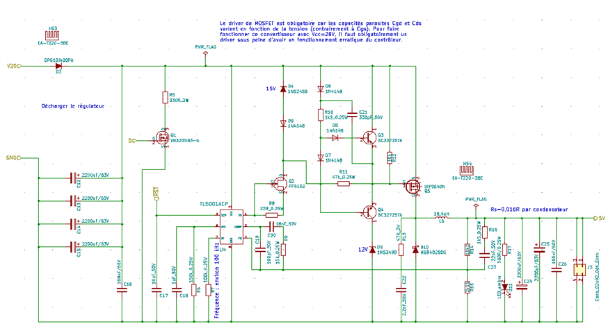
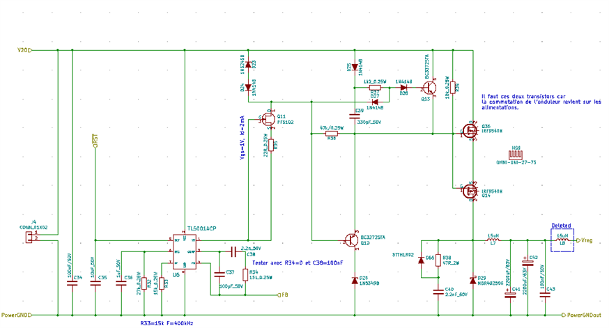
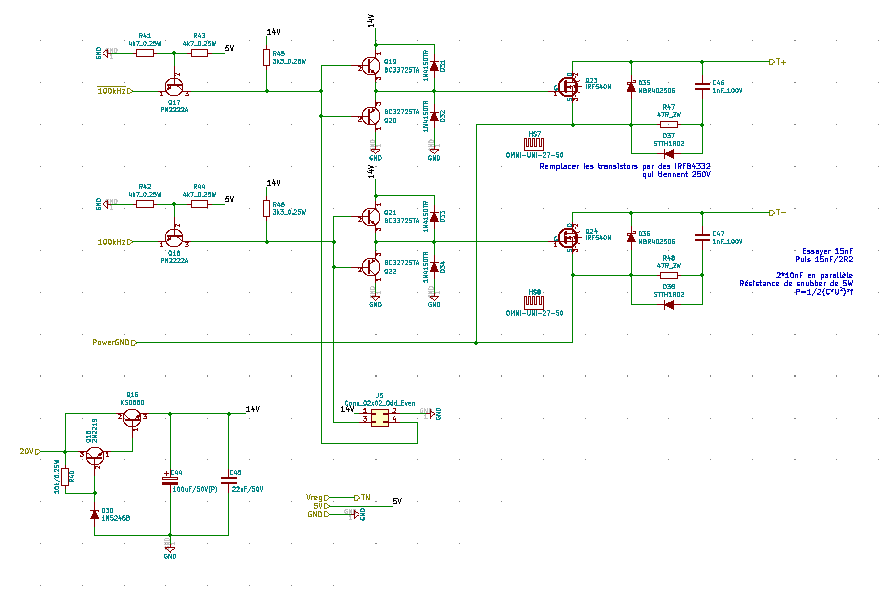
Channel 1 (bottom) is main output (value on multimeter). Expected value is 412Vdc.

Channel 2 (top) is feedback signal (TL5001A pin 4).

You can see that TL5001A continuously starts and stops and feedback signal is not equal to 1V. This signal varies between 0.75 and 2V.

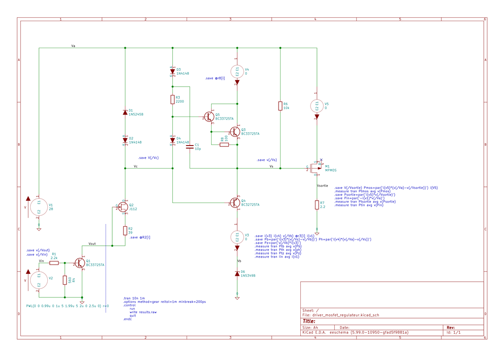
I can repost here actual design if required, but some information are available on old thread : https://e2e.ti.com/support/power-management-group/power-management/f/power-management-forum/991873/tl5001a-tl5001a-compensation-network/3666902

Best regards,

JB

  • Hi JB,

    Thank you for coming back.  Lets do the debugging step by step. 

    I would like to check your gate drive circuit.  Could you remove the MOSFET, and just operate with the TL5001 by supplying the input voltage, and monitor the OUT pin and your driver signals, to see if the driver is operating as expected? 

    If yes, then we need to put back your FETs.  To my understanding, the driver voltage should be applied across the MOSFET G and S, but your circuit does not seem doing so. Could you try first to delete  Q14 and short  its D-S pads on your circuit?

    Thanks,

    Youhao

  • Which MOSFET ? Q36 and Q14 ?

    To be honest I use the same driver for very long time when I use a TL5001A. This driver comes from datasheet (or application design, I don't remember) and it run as expected. For example, exactly the same driver is used to generate 5V from V20 (28V). Nevertheless, I will try to check gate signal.

    Schematic of a running 5V converter:

    Last converter runs as expected and I have tested it with an electronic load until, if I remember, 12A.

    Converter for high voltage is:

    In this schematic, only Q14 is mandatory. This converter runs at 400 kHz. Don't remember that Vreg enters in a inverter (that runs at 100 kHz). Q36 isolates V20 from Vreg when Q14 is switched off. Without Q36 (my first PCB did not have Q36), V20 is scrambled by the switching of inverter by the body diode of Q14.

    Best regards,

    JB

  • Hi JB,

    Sorry for the typo: I meant to short out Q36.  In a buck circuit, the body diode of Q14 should never conduct because it is always reverse biased.  Please refer to Figure 21 of the datasheet.  

    Thanks,

    Youhao

  • The first version of this circuit doesn't contain Q36. Please don't remember that Vreg is connected to a inverter that contains a transformer.

    Transformer is connected between T+ and TN (=Vreg), and TN and T-. Commutations can given overshoots on Vreg (80 V during a few µs). I have added a snubber circuit to reduce these overshoots but I'm not able to avoid these overshoots due to recovery time of D37 and D38.

    Without Q36, these overshoots return to V20 though body diode of Q36 that is directly biased!

    There is only one difference between drain and source of a mosfet transistor: anode of body diode is always connected to drain. Thus, with Q14 and Q36, I create a new component that is equivalent to Q14, but without its internal body diode.

    Regards,

    JB

  • Hi  JB,

    The circuits that you showed earlier were buck converters, and what is the topology of last circuit where you haven't show the transformer but just the two terminals of the transformer?  

    By the way, just another opinion to share: without the Q36, the body diode actually works as a clamp to prevent the switch node voltage from spiking too much, and part of the energy actually returns to the input line rather than dissipated in the circuit.  You may reconsider the use of the snubber and Q36.  

    Thanks,

    Youhao

  • Hi Youhao. I will try to send to you as soon as possible some waveforms but I have for several days a lot of other projects on my desk.

    Best regards,

    JB

  • Hi Youhao.

    I took some chronograms.

    First one : Vgs voltage (Q36). Volmeter shows output voltage (expected value: 412Vdc).

    I have to improve driver with Spice. This driver was optimized when it ran @ 100 kHz. Now, it runs @ 400 kHz. @100 kHz, Vgs varies between 0V and -14V. Please note that when I took these chronograms, no load was connected to output power.

    Now, feedbak signal is:

    Vfb shows a lot of spikes (between 0.6 and 1.4V), thus, TL5001 continuously starts and stops...

    Best regards,

    JB

  • Hi JB,

    We will study this and get back to you by next Tue.

    Thanks,

    Youhao

  • Hi JB,

    The driver signal appears weak because its falling edge is slow meaning a weak driver to drive the PFET.  The falling edge should be steeper to make the pulse to be more closer to an inverted square wave.  Such a slow driver would cause more switching losses, and also reduce the effective duty cycle.  Please adjust your driver to be stronger.

    Thanks,

    Youhao

  • Hi Youhao.

    I don't agree with you. I have done this morning some Spice simulations to have a good idea of different signals.

    In a first time, here is my driver:

    M1 is an IRF9540. With R7=1R, M1 efficiency is about 87%. If R1=2R2, this efficiency is about 92%. With D6.Q3.Q4, this efficiency is greater than 90%. Don't forget that IRF9540 is switched on in less than 170 ns (Vgs = 6V is enough in my case). Vgs = 10V in 320 ns.

    Result of simulation:

    If you know how to optimize this driver, please give me improvement I can add. Please note that result of simulations strongly look like real signals.

    That being said, a weak driver cannot explain what I seen in feedback loop.

    Best regards,

    JB

  • I have fixed schematic TI provides in its application design. With the following circuit, efficiency between input and output is equal to 93.5%. But it doesn't fix oscillations.

    Fall time (0 to -10V) : 90ns

    Rise time (-10 to 0V) : 130ns

    If I replace C1 by 330 pF, rise time is reduced but current in Q3 reaches 1A when M1 is switched off.

  • Hi JB,

    Your scope picture does not show 170ns  nor 390ns, but a much longer time. Anyway, we may also need to adjust the loop compensation.   In your new schematic you just shows a FB node feeding to the FB pin, but how this FB is generated from the output rail is not shown.  In your previous design you did show the entire FB circuit from the output rail to the IC pins.  Could you also share the entire FB circuit in this new design?

    Thanks,

    Youhao

  • Hi Youhao,

    I have uploaded my design here : hilbert.systella.fr/.../alimentations_haute_tension.pdf

    This design uses two TL5001A, the first one runs as expected and provides 5V for this PCB and some others. The second one is on sheet 7/9, followed by an inverter (9/9) and rectifier (4/9).

    Regards,

    JB

  • Hi JB,

    Just let you know that I am still studying your schematic.  Since the circuit are spread on different pages, it takes time for me to trace the signals on the computer display.  Page 1 shows a push-pull stage is inserted between the TL5001 dc stage output (page 9) and the regulated rail (Page 4).  My understanding is that Push-pull must be implemented with current mode control or the transformer saturation can easily occur, and hence the instability issue which cannot be fixed by the loop compensation.  I am afraid this may be one reason for the issue but I might be wrong.  Have you done similar design before that worked without problem? 

    Thanks,

    Youhao 

  • Hi Youhao,

    Each half transformer presents L=15 µH, but I don't know how compute saturation current. Transformer is made with https://www.digikey.fr/product-detail/fr/epcos-tdk-electronics/B64290L0659X087/495-5084-ND/3913578

    I have done a long time ago some similar designs that ran as expected but at lower frequencies and lower output voltages.

    Best regards,

    JB

  • Hi JB,

    I am still working on analyzing your circuit, and I should get back to you next week.  Sorry for the delay.

    Thanks,

    Youhao

  • Hi Youhao,

    No problem.

    Regards,

    JB

  • Hi JB,

    Very sorry for the delay.  This took me awhile to trace the signals. Could you try the following to see if there is any improvement:

    • Please short Q36 for the test.
    • Assume L8 is shorted and C59 not used as your schematic markup.
    • Change R34 to 3.3k
    • Change C38 to 100nF
    • Change C37 to 1nF

    If you don't see the improvement, please tell me the part numbers or share the datasheets of C41, C42, and C53-55. 

    Best Regards,

    Youhao

  • Hi, JB,

    I pulled the circuit in 7/9, 9/9 and 4/9 together, it forms a push pull circuit operating at 100kHz, 20V to 400V conversion. Please correct me if these data are not accurate.

    Based on this circuit, intrinsically, there are two issues that are concern:

    1. grounding issue: we must carefully avoid grounding noise. Otherwise, signals will be lost/compromised in noise.

    2. clear feedback signal sensing: how to make sure the signal on FB pin is clear and stable accounting for the fact that feedback signal amplitude is as low as 1V? especially you pull the FB signal from far away (maybe from another board)

    I suggest you use large cap to stabilize the FB signal first.

  • Hi Youhao,

    I will test next monday.

    Best regards,

    JB

  • Hi Zhiyang,

    There is no grounding noise. feedback is pulled from the same board.

    I have tried to add a large capacitor  between FB and ground without better result (R56/R55/C56 is a high pass filter destroyed by this capacitor). Maybe with a AOP (follower amplifier) between compensation network and high pass filter ?

    Regards,

    JB

  • Hi, JB,

    Then go ahead to do test as suggested by Youhao.

    Thank you.

    Zhiyang

  • Sorry Youhao, I have a lot of work and I haven't tested. I will do some tests this week. I hope.

    Best regards,

    JB

  • Hi JB, 

    Understood that you have been busy.  We are looking forward to your test result, for we are also eager to know if it works or not. 

    Best Regards,

    Youhao

  • Hello Youhao. I beg your pardon, but I have no time to test until 15th of august. I'm not sure this topic will remain opened. If not, I will come back in a new topic with result of my tests.

    Best regards,

    JB

  • Hi JB,

    Understood.  Let me close it here for now and you are welcome to reopen it or create a new post. 

    Best Regards,

    Youhao