This thread has been locked.

If you have a related question, please click the "Ask a related question" button in the top right corner. The newly created question will be automatically linked to this question.

TPS63031: No-load operation of TPS63031

Part Number: TPS63031
Other Parts Discussed in Thread: TPS63030

Hi.

I have a problem with the development of our product, more precisely, with the operation of the AT42QT1012 touch chip.

We have our engineering design for a wearable device that has an AT42QT1012 Touch sensor chip. All-time MCU, LCD is disabled. The user can enable the device by the touch sensor. After enabling the system must shut down by itself within 15 minutes (+-10% according to datasheet).

The problem is that the current design doesn't work stably: the device is enabled by itself: when I leave the system on the table, the PCBA is connected to the battery, without any action, or put it on the charge, periodically, the touch turns on and off itself, without my participation.

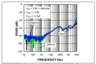
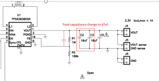
In our previous PCB design, the touch worked perfect, but the DC / DC consumed a lot of current. We corrected the design of the DC / DC connection (like described in this post: https://e2e.ti.com/support/power-management/f/196/t/962067), added several resistors '0' so that it was possible to disconnect components from the PCB. Now DC / DC does not consume current, but the touch began to turn on / turn on itself. In the previous PCB design the DCDC out was like an attached image 2 all time.

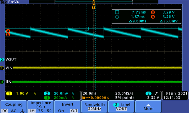
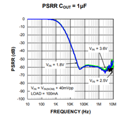
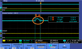
But now, when the DCDC is in "Power Saving Mode", it works like an attached image 1.

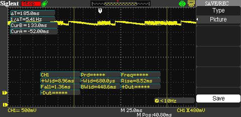
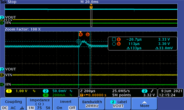
When touch is "ON" and the system starts operation, the DCDC outputs exactly 3.3 volts DC, like an attached image 2.

This answer I have received from Microchip:

"If there is considerable noise in the power supply, such behavior can be observed. As the touch technology charges the sensor and measures the charge stored, any fluctuation in the voltage during this charging and measuring process can affect the signal values which can be similar to a touch (that changes capacitance).

Hence such false detects could occur."

How can I resolve this issue and equalize the voltage: remove the waves?

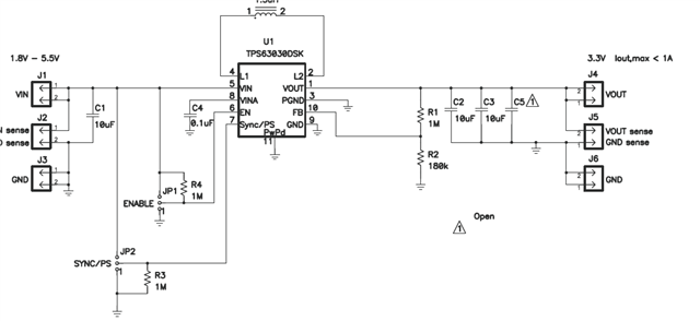
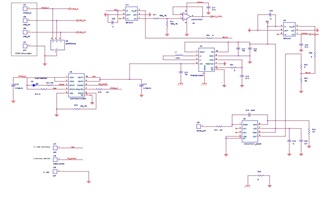
Attached my power management side schematic:

Thanks

Evgeni

  • HI  Evgeni,

    thanks for your detailed description.

    could you help to confirm questions as below:

    >>>false detects are  trigged by high frequency noise as red part or the low frequency ripple  as blue part?


    >>>high frequency noise in red circle is caused by what?  I do not think it is caused by PFM mode.

  • Hi Tao.

    I don't know when occurs false triggers, in a red part or in a blue part. I don't know what gives the noise in the red circle. According to the "IQ - What it is, what it isn’t, and how to use it" document, TPS63031 works in the Power Safe mode ( No-load operation).

    Can you give me any advice to understand how to remove the noise in Power Safe mode?

    Thanks.

    Evgeni

    IQ - What it is, what it isn’t, and how to use it.pdf

  • Hi  Evgeni,

            I am not sure  the high frequency noise in red part is caused by what, i am sorry i can not give your advice actually,  increase the output capacitor may help.

            But the low frequency ripple is caused by Power Safe Mode, it is decided by internal of TPS63031, is it possible make TPS63031 work in force PWM mode by connect SYNC pin to VINA in your application?

             Here is some other advice for you:

     >>>make sure  false detect is triggered by what? it is very important.

     >>>If the false detect is triggered by TPS63031, find out which part, high frequency noise or low frequency ripple?

     >>>If it is caused by low frequency ripple and FPWM mode is not allowed. It seems that you should try other solution.

     >>>power AT42QT1012 with DC source  to make sure the false detect is caused by TPS63031


  • Hi Tao.

    I disconnected the touch from the DCDC and connected it directly to the vbat of the charging chip (it gives out the battery voltage all the time from 3.3 to 3.7 volts, depending on the battery charge level. After that, the touch stopped spontaneously turning on and off. This means that the saw that the DCDC makes in the energy-saving mode starts the touch.

    What is the solution to use DCDC in energy-saving mode, but without the saw?

    Thanks.

    Evgeni

    Attached picture from other PCBs (without red noise, but with the same reaction).

  • Hi Evgeni,

         thanks for your trying, is it possible to increase the effective output capacitance  value? It may help

         BTW, could you help to ask the acceptable value of output ripple?

         I will do some try based EVM.

  • Hi Tao.

    Ripple voltage on the power supply should be less than +/-25mV.

    What is means "increase the effective output capacitance value"?

    Evgeni

  • hi Evgeni,

         capacitance will change with DC bias as curve below, this curve is depend on the  material  of capacitor and temperature.

         BTW, increase the output capacitance is helpful to decrease the ripple voltage in my test.  hope it will solve the issue


  • Hi Tao.

    Can you describe what you did in the test to decrease the ripple voltage in the test? Which capacitor has changed to which capacitance in the schema?

    Evgeni

  • Hi Evgeni,

          I am sorry, I missed C19 C35 in your schematic and output capacitor is larger enough to decrease the  ripple voltage.

          It seems no method to  solve this problem based TPS63031 except FPWM mode is acceptable   


          I tried another solution TPS63030, it has no different but output voltage be set by resister divider with TPS63031.

          test condition: 27pF capacitor in parallel with R1    total capacitance of C2 C3 change to 47uF. 

          Schematic is attached as bellow:


        Test results: ripple of output voltage is 35mV,   a smaller one will get if you increase the capacitor in parallel with R1 or C2 C3.

                             loop is stable too in the test.                                   

    so if it is possible change solution to TPS63030? the datasheet is attached

              tps63031.pdf

  • Hi Tao.

    1. What is the "output capacitor", C12 or C13 in my schematic? What is a possible step for increase its value?
    2. Is possible to enable FPWM in Power Save mode for TPS63031? How can I do this?
    3. What is a spike in the last picture? Is possible to remove it? What is the current TPS63030 consumption in the power save mode, less than 50 μA?

    Evgeni

  • HI Evgeni,

         1.C19 C35 C12 C13 are output capacitor in your schematic, may be you change C12 C13 to 22uF.

         2.connect PS pin to VINA pin, Then TPS63031 will work in FPWM mode

         3.Spike in the last picture is caused by load transient, it will not exist in steady state.  The current TPS63030 consumption is same as

    TPS63031 in the power save mode and it is depend on the load, such as  leakage current of component and operating current of AT42QT1012.

  • Hi Tao.

    1. Will installing a Ripple blocker help eliminate, smooth out or limit ripples so that they are within 5-15mV? Like 

    https://www.microchip.com/ParamChartSearch/chart.aspx?branchID=chartno_742 This is not TI. You can propose your chip. I need to resolve this issue.

    2. What is the current consumption in the FPWM mode? In Datasheet no information about this. How can I configure 100% duty high (without ripple)?

    Evgeni

  • HI Evgeni,

         Unfortunately,  Ripple blocker have no help to low frequency ripple, as showed in the PSRR curve.

         If adding a Ripple blocker is acceptable, do we have a chance to change solution with TPS63030? 

         The total consumption can be calculated by equation:  P=Vout*Iout/EFF (where Vout=3.3V; Iout means the operation current of  AT42QT1012 and some leakage current, I think the leakage current is smaller than 1mA; EFF can be found as blue curve below).

        or else, could you show me the operating current of  AT42QT1012 and input voltage of TPS63031?  I will have a test with EVM board


        hope every thing goes well.       

  • HI  Evgeni,

            I am sorry for check some part number in your link.  it also contains some products with high PSRR in low frequency and seems able to solve your problem.

            BTW, have the problem solved already?  

    Best regards

    Tao

  • Hi Tao.

    I haven't a development board. I am currently looking for 0402 capacitors for replacement in my PCBs instead of C12 and C13 to 15uF, 18uF, 22uF, 27uF for reducing ripple, like in your test result.

    Can you explain in more detail what you mean: "it also contains some products with high PSRR in low frequency and seems able to solve your problem."?

    Thanks.

    Evgeni

  • HI Evgeni,

          With smaller package and larger capacitance, effective capacitance may decrease for  rated voltage reduced or worse material(such as X7R change to X5R). please be careful. 

          such as 94325/45/55, PSRR curve is attached below.      


         you can also find many similar chips in TI.com, such as TLV73333P.

         Notice: consumption will higher with added LDO for efficiency decrease

  • Hi Tao.

    I have received the capacitors 15uF and 27uF and replaced them on my PCBs (you can see in the image). I don't see any ripple updates when DCDC is running, unlike your image from 09 Jun 2021.


    Can you propose to me any suggestion from a TI representative to find a decision and solve my problem?

    I must use stable 3.3V in Power Save and Work mode without a ripple.

    Thanks.

  • Hi Evgeni,

          Thanks for your trying. please notice that test is based TPS63030 but not TPS63031, and a feedforward capacitor is added in paroral with R1.

          could you show me more details about "without a ripple"?  +/-25mV is ok?  I will have a discuss with colleagues.

    Regards

    Tao

  • Hi Tao.

    Where can I buy a development board with TPS63030 that you used for experiments? Give me the link, please. I want to try to get the same result as your one (this is your picture).

    Thanks

    Evgeni

  • Hi Evgeni,

            you can buy EVM with follow link, please check.           

            https://www.ti.com/tool/TPS63030EVM-417?keyMatch=&tisearch=search-everything&usecase=partmatches

            By the way, waveform attached in you latest reply is a transient test to make sure loop is stable. please take follows as reference.


    Regards

    Tao     

  • Hi Tao.

    Thanks for the link.

    Can you check on your development board, if there are spikes that we can see in the picture all time, or periodically, or sometimes?

    In addition, is possible to use PSpice for TI Simulator for these tries instead to try to replace capacitors in the Dev Board? www.ti.com/.../PSPICE-FOR-TI

    Thanks

  • Hi  Evgeni,

           you are welcome.

           Spikes only appear during transient load switching, output current change to 0.1A from 0.5A with 250mA/us. I want  to confirm that my changes will not affect the loop stability by this test. I'm sorry for confuses you with this unnecessary information.

           That is a good idea of PSPICE, But you may need some time to adapt to this software. Simulation and actual measurement results may have some slight differences due to parasitic parameters, but the overall trend is the same. 

    Regards

    Tao


  • Hi Tao.

    "Spikes only appear during transient load switching, output current change to 0.1A from 0.5A with 250mA/us. I want to confirm that my changes will not affect the loop stability by this test. "

    I want to clarify for myself:
    1. This picture shows how DC-DC works in Power Saving mode.
    2. This means that in Power Saving mode no spikes? This is important because this spike can interrupt the touch (spike > 0.25mV).
    3. Can you provide me with a schematic connection of DC-DC TPS63030 and your capacitors and resistors changes so that it can work in energy-saving mode, as in the last representation (but without spike):

    • automatically switch to operating mode (DC 3.3 volts) after touching the touch and turning on the SIP.
    • automatically switch to Power Saving mode after turning off the SIP and all PCB periphery is disabled.

    4. According to the TPS63030 Datasheet, "the converter stops operating if the average inductor current gets lower than about 100 mA". This value is the same as in TPS63031. My PCB in operation mode work between 90mA up to 110mA. Could it happen that DC-DC will not work according to my scenario, but will go into Power Saving mode because the current consumption is below 100 mA?

    Thanks.
    Evgeni

  • Hi  Evgeni,

         Maybe  I didn’t explain clearly enough, i would like to explain for you again  as follows.

         1.This picture is taken in PWM mode with a transient to make sure loop is stable. it has nothing to do with PFM mode. As you know, loop test is meaningless in PFM mode for a bigger ripple is exist and loop is not same with PWM mode. 


       2.This picture is taken in PFM mode, a low frequency ripple 35mV is exist in the test. I prefer to call high-frequency signals "spikes" while low-frequency signals "ripple". I am sorry it makes you confused


       3.Here is the schematic in the test . please notice the red part 


       4.Yes, if tps63030 work in buck topology, for output current is same as average of inductor current, it may run in PFM mode, but ripple will much smaller. ripple is different with different output current.

           If work in boost/buck-boost topology. output current is smaller than average of inductor current.

           so I think it is ok with your application.

  • Hi Tao.

    Is it in Power-Save mode TPS63030 works in PWM mode or in PFM mode? What is PFM mode? I don't see any information in Datasheet about this.

    Can you provide 2 measurements with TPS63030, please:

    1. In Power-Save mode (without ripples and spikes). What is the consumed current?

    2. In Operation mode (without ripples and spikes). 

    The ripple voltage on the power supply should be less than +/-25mV in both cases. Otherwise, this DC-DC is not suitable for our system.

    Thanks

    Evgeni

  • Hi  Evgeni,

        For part of our instrument was sent for calibration yesterday, there will be some delay for my test. I hope to give you a complete and detailed      test report before next Wednesday, is that ok?

        I think you can take follow picture as PFM mode, but it will be some different with TPS63030.


    Regards

    Tao


  • Hi Tao.

    I understand. No problems. Will wait for your test report.

    Thanks and best regards.

    Evgeni

  • Hi  Evgeni,

     thanks for your tolerance,  please check the attachment and hope it will help your case.

    ways to decrease output ripple of TPS63030 during PFM work.pptx

  • Hi Tao.

    Thanks for your measurements. What do both measurements mean? At what outlet are green and crimson colors measured? 

    The system must work in the Power Save mode without ripples. What are these ripples?

    Is TPS63030 can work like in your picture but without spikes? Is PWM mode allow in the Power Save mode?

    Thanks

    Evgeni

  • Hi  Evgeni,

    What do both measurements mean? At what outlet are green and crimson colors measured? 

    green: inductor current    crimson: output voltage.   just zoom in from another. i want show you how PFM working 

    Is TPS63030 can work like in your picture but without spikes? Is PWM mode allow in the Power Save mode?

    Do you mean with light load? Then you should choose FPWM mode.  

    Working state will change from PFM to PWM if load increase in Power Save mode

  • Hi Tao.

    Can you provide two measurements with TPS63030 when it works in FPWM, please:

    1. In Power-Save mode (without ripples and spikes). What is the consumed current?

    2. In Operation mode (stable 3.3V without ripples and spikes). 

    The ripple voltage on the power supply should be less than +/-25mV in both cases. Is this possible?

    Thanks

    Evgeni

  • Hi  Evgeni,

          Do you mean have a consumed current test both in PFM/PWM mode(make sure ripple is less than ±25mV) without  load?  

    regards

    Tao

  • Hi Tao.

    This means that I want to see the possibility DCDC do ripple in Power Save mode up to 25mv without spikes. Is this possible?

    Evgeni

  • Hi   Evgeni,

         Yes, of course.  as shown in page 20/21/22 of the attched PPT. output ripple is smaller than 25mV without spikes.Do you have questions about the results of this test?

    Regards

    Tao

  • Hi Tao. 

    I have found the problem in my design. I turned off the DC-DC completely and used a Low-Dropout Voltage Regulator to stabilize the voltage. Everything worked as it should.

    Conclusion: the noise generated by the DC-DC in the power saving mode does not allow the Touch chip to work stable.

    Thanks a lot for your help and patience.

    Best regards.

    Evgeni

  • Hi   Evgeni,

        Great!!!  have a nice day. let us keep in touch.

    Regards

    Tao