This thread has been locked.

If you have a related question, please click the "Ask a related question" button in the top right corner. The newly created question will be automatically linked to this question.

BQ76942: MOSFET Driver

Part Number: BQ76942

Hi Matt, Terry,

When I debug the BMS, I meet a MOSFET driving issue. That is I have secondary protection IC, and if AFE fails, the secondary protection IC will pull down the MOSFET driver pin directly.

The schmatic is shown as the below picture. I use a 2K resistor(R1) to connect bwtween the DSG pin of BQ76942 and the Gate drive point(shown in the picture in red).

If the secondary IC proecction happens, it will pull the point Gate drive to ground via a N-mosfet.

My question is if the Gate drive point is pulled down to the ground, the DSG mosfet driver current will all flow via the R1.

Will this design damage the mosfet driver of BQ76942?
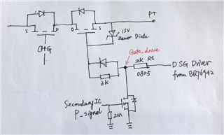
 

BTW, is the mosfet driver of BQ76942 a voltage source or a current source? If it is a current source, how much is its current value?

If I don't pull down to the ground, but with a resistor between the pull down mosfet and Gate drive, what value should I choose the resistor? Will it turn off the DSG fet completely?

Thank your for your help.

  • Hi Sean,

    The pull down MOSFET must overcome the charge pump output with some margin.  When pulling down CHG (which is not your diagram) 200 uA may be sufficient.  The charge pump is common between the drivers, so if you pull down CHG you will also pull down DSG, but pulling DSG to the BAT voltage will not turn off the DSG FET, just limit its gate voltage.  So you will want to disable the DSG drive also.

    In your diagram the external control MOSFET pulls down the discharge gate.  The DSG driver is a voltage drive but has a current limit when pulled down, about 10 mA, but that is not a data sheet parameter.  So provide good margin in your FET.  Your FET will pull the drain node to 0V.  The current from the DSG pin might be 10 mA, so with your 2k resistor the DSG voltage might be 20V, or somewhere less than the BAT voltage.   No damage is expected from the current from DSG.  Plan for the power in the resistor.

    With the external MOSFET drain pulled to 0V the gate of the discharge power FET will be pulled down below P+.  A load on P+ will bring down the P+ voltage, or the Zener diode will conduct discharging P+ through the Zener and the other 2k resistor shown.  If the system user connects a 40V charger to the P+ with the clamp MOSFET on, again plan for the power in the resistor 

    If you put a resistor in the drain path of the clamp MOSFET it will have a voltage drop from the current out of the DSG pin (and out of P+ as it discharges).   If the voltage drop on that drain resistor (not shown in the sketch) were 5V and Vgsth of the discharge FET were 3V, you would have 2V on P+ and the battery would still deliver current to a load at the low voltage.  So be sure a drain resistor provides less than Vgsth of the discharge power FET.