This thread has been locked.

If you have a related question, please click the "Ask a related question" button in the top right corner. The newly created question will be automatically linked to this question.

BQ76PL455A-Q1: Communication initialization

Part Number: BQ76PL455A-Q1
Other Parts Discussed in Thread: BQ76PL455EVM

Hello,

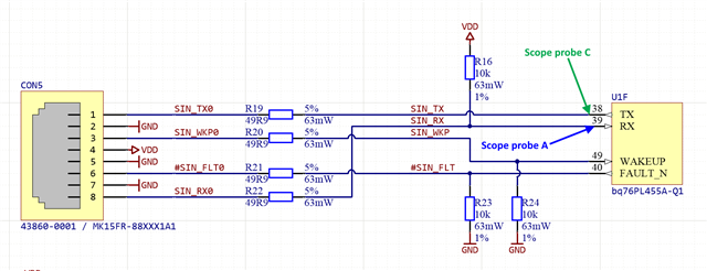
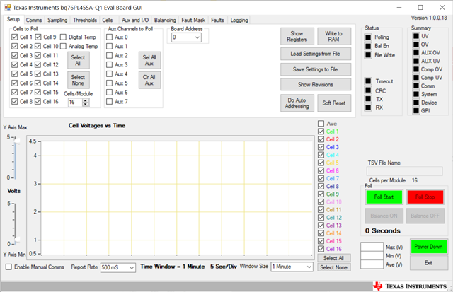
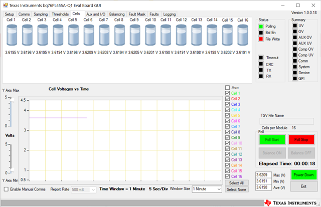
I have designed a custom board based on the bq76PL455A-Q1 device and the bq76PL455EVM evaluation module. I am now trying only with one board to communicate it with the host PC over an FTDI USB to UART adapter and the TI DEMO GUI app. The communication scheme of the "master" device looks the following:

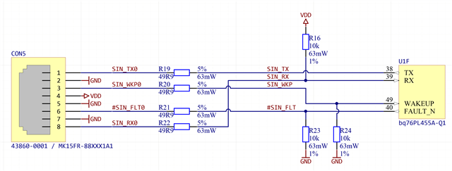
Currently only the TX and RX pins are connected to the adapter. The power management part looks the following:

Each bq76PL455A-Q1 board is a "slave" by default. If the USB adapter is connected to the master connector, the 5V power logic is applied from him to the VIO port, which overlaps the on board 5.3 V from the LDO (the D7 voltage drop is ~0.5 V so no conflict between the on board LDO and ext. power supply).

I have observed the following behavior so far:

  1. After the bq76PL455A-Q1 board is connected to the cells (no ext USB adapter yet), the VP voltage is not present. Only the V5VA0 is present (~4.8 V), Here I assume that the IC is the the SHUTDOWN mode by default.
  2. After I short the V5VA0 with the WAKEUP pin for a sec, the VP appears for couple minutes (here I assume that the device went to IDLE state). The V5VA0 goes 5.3 V as well from 4.8 V.
  3. If instead I connect the external USB->UART adapter (which applies 5V to the VIO) the same happens- the voltage on VP appears (~5.3 V). Here I also assume that applying voltage to VIO wake up the device.
  4. So now I have the VP voltage present and my USB adapter connected (only 5V, GND and TX/ RX signals present). WAKEUP and #FAULT are not driven, so they are in the default state and pulled down via resistors on board.
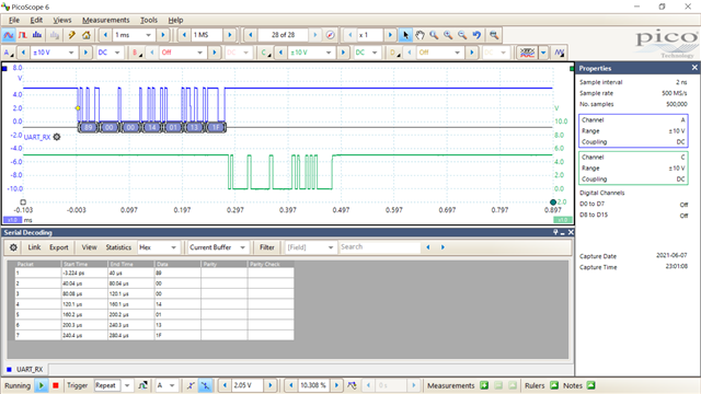
  5. I open the bq76PL455_GUI application, choose the right port and press OK. Few things happen now:
    1. An error is shown saying "Unable to open com port",
    2. On the USB to UART adapter I can see that some data is transmitted (TX led blinks), but no data received (RX led is off),
    3. The VP voltage drops to around 1.2 V. The only way to make it go back again, is to disconnect the USB adapter and the power from VIO and reapply it again (or apply level high on the WAKEUP pin, but wont work is VIO is not reapplied).

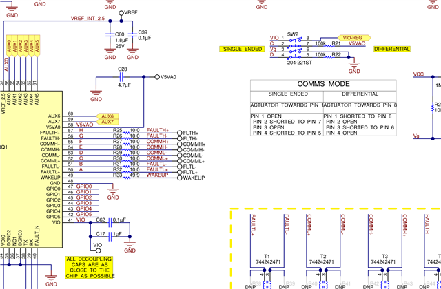
So to summarize, it seems that some internal states of the bq76PL455A-Q1 are changing, but I cannot communicate properly with the device. What am I doing wrong in here? Am I missing anything in the hardware? I have studied the EVM board design again and the only real difference in HW for the master device I could spot is that the COMML+/ COMML- lines are pulled up/ down with 100k resistors- but can this be the case? Also instead of completely disconnecting the regulator output, I have the D7 diode, but in this case it does not conduct, as the 0.5 V voltage drop is not reached (regulator output is 5.3 V, the applied VIO externally voltage is 5 V). 

I would appreciate all help, as I am struggling with this for many hours now without any resolution...

  • Hello Lukasz,

    Can you please follow all the steps from this similar debug thread and let me know if anything helps: You are using the exact FDTI ttl-232r-5v cable right? It cannot be another part variation and needs to be updated with proper drivers from FDTI website first.

    https://e2e.ti.com/support/power-management-group/power-management/f/power-management-forum/655494/bq76pl455evm-bq76pl455evm-unable-to-open-com-port 

    Can you also send measurements for all below voltage rails?

    VIO = 

    VDIG = 

    V5VA0 = 

    VM =

    CHP = 

    VREF =

    VP1 = 

    TOP =

    TX = 

    RX = 

    Regards,

    Taylor

  • Hi Taylor,

    Thank you for the answer. I have read the posts from the topic you have linked. It seems that the UART #CTS and #RTS lines are somewhat used in a "hacky" way with the EVM. I do not have the exact cable specified in the EVM DS, but I do have a legitimate FT232 based USB adapter that has RTS and CTS exposed as well. I haven't installed any special drivers though.

    Before I dwell further into the details, let me star of by saying that my adapter is sending data when the GUI program starts and that can be observed on the scope:

    The data is visible on the RX line (have set the serial parser to 250k, 8 bits, 1 stop bit, no parity).

    First program open:

    Second program open:

    I assume the transmitted data by the program is correct, but there is no response from the bq chip. 

    In my config, only the VDD, GND TX and RX lines are connected. The WAKEUP and #FAULT are floating. If we examine the information gathered about the connections, it could be setup together like this:

    So it seems that the #fault drives the #CTS pin, while the #RTS signal (on the host side) drives the WAKE pin, which's logic is flipped on the EVM PCB. On my HW, the WAKE input is not flipped, so I have changed the logic of the RTS pin in the FT_PROG (its now low by default). This allowed me to communicate with the device from the host PC!

    The question I have now is: how does the initialization of the communication protocol work actually? I could not find this information anywhere and I need to implement this functionality into the host MCU...

    Thank you for the answer again Taylor and I would appreciate your further feedback.

  • Hi Lukasz,

    Unfortunately I don't know what to expect if you don't use the exact FDTI ttl-232r-5v  cable and updated drivers as spelled out in the GUI user guide. As for initializing the comms, you may want to refer to our MCU code and associated documentation below. Essentially, you will need to 1) wakeup 2) autoaddress 3) begin write/reads

    https://www.ti.com/lit/an/slva617a/slva617a.pdf 

    Regards,

    Taylor

  • Hi Taylor,

    I think for the serial cable part we are good now. I should now have the same config on my side.

    The problem is with the initialization sequence. The mentioned by you document is not very rich in explanations on this part:

    I still do not know how should the communication initialization look like in terms of WAKEUP pin and its timing (for how long should the pin be set high and in what time should the first message come to the bq IC).

    Thank you and I would appreciate your further feedback.

    Lukasz

  • Hi Lukasz,

    This part from datasheet explains WAKEUP 0 - 1- 0 transition and timing, and delay before auto addressing commands after this. The example code also has this written out.

    Regards,

    Taylor

  • I can work with that, thanks!