This thread has been locked.

If you have a related question, please click the "Ask a related question" button in the top right corner. The newly created question will be automatically linked to this question.

TPS25947: RPW0010A UltraLibrarian Footprint still isn't right

Expert 2031 points
Part Number: TPS25947

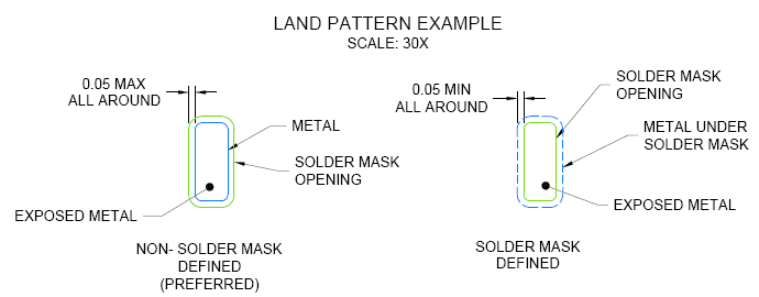
It doesn't look like the Altium UltraLibrarian footprint for the TPS25947 has been fixed.  The datasheet shows the correct solder mask information.  In the Altium UltraLibrarian footprint, the solder mask is exactly the same size as the copper pads.  Here are some screenshots:

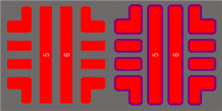
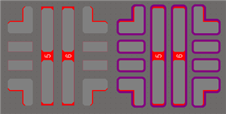
The UltraLibrarian footprint is on the left, and what it should look like is on the right.

Copper pads, with solder mask in the background:

Solder mask only:

Copper, solder mask, and paste layers:

Greg

  • Hi Greg,

    Altium footprint is following solder mask defined pattern so solder mask openings is not beyond the metal. The datasheet shows both options solder mask defined and non solder mask defined. Is non solder mask defined better?

    Regards

    Kunal Goel

  • Hi Kunal,

    The footprint is not following either option, though technically you could say it is following non-solder mask defined per the datasheet.  I say that because the datasheet says "0.05 MAX ALL AROUND", so technically 0.00 meets the requirement (but is not a good value to use).

    Per the datasheet, Solder Mask Defined requires an overlap of at least 0.05, but the solder mask and copper in the UltraLibrarian footprint are exactly the same size.

    You should not have a solder mask that is exactly the same size as the copper pad.  It is virtually impossible to align the solder mask with the copper perfectly.  You will have solder mask partially on the pad.  I've been told this tiny amount has a tendency to flake, and you don't want pieces of solder mask ending up elsewhere in another solder joint.  Non-solder mask defined is preferred because the solder has more surface area to attach to, providing a more secure attachment.  This is especially true because the attachment is in multiple dimensions because it attaches to the sides of the pad as well as the top.

    The reason there is a MAX spec for Non-Solder Mask Defined is because you need a minimum amount of solder mask web between the pads.  Otherwise the web can break and flake off and become a problem elsewhere.

    Regards,

    Greg

  • Hi Greg,

    Thanks. Got your point. I will check with team if we can get this updated.

    Regards

    Kunal Goel

  • Hi Greg,

    I checked with our team creating these parts. It is TI guideline that  solder mask layer will identically match the copper layer. Any further query you have?

    Regards

    Kunal Goel

  • Hi Kunal,

    Thank you for contacting them.  I believe there is inconsistency then.  I just randomly chose a different footprint to download (DBV0006A), and the solder mask expansion is set to 2 mils.  I think 2 mils is a reasonable value.  If it is TI's guideline to make the solder mask identical to the copper layer, then why isn't it done that way for DBV0006A?

    Regards,

    Greg

  • I just asked the PCB fabricator that I usually use about this and this was his reply:

    "If we were sent mask pads same size as copper pads, engineering would reject it in our DFM and ask if they can increase the mask.  If you insisted we build it to the Gerber file, they would specifically ask you for approval to allow mask encroachment on pads".

    Are you sure that your team is not confusing paste with solder mask?  The paste layer is usually 1:1 with the copper.

    Greg

  • Hi Greg,

    Can you share footprint you downloaded? No Greg I have checked they are not confusing paste with mask. Can you get the altium footprint modified? I think when you download UL file from ti.com it has a text file in it ,in which you can do the edit.

    Regards

    Kunal Goe

  • Hi Kunal,

    Which footprint are you referring to?  RPW0010A or DBV0006A?  They are both directly off the TI website. This is the DBV0006A I downloaded: https://www.ti.com/product/SN6505B?keyMatch=SN6505B&tisearch=search-everything&usecase=GPN#design-development##cad-cae-symbols

    I would like to understand TI's rationale for defining a solder mask expansion of 0.  I've done some research this morning and the best I could find is one site (Sierra Circuits) that said fabricators prefer a 1:1 match so that the expansion can be altered to the appropriate manufacturing process.  Strangely, I've never encountered that before, but I have had PCB manufacturers alter my solder mask openings.

    Regards,

    Greg

  • Hi Greg,

    TI idea is similar. We are giving the customer flexibility to adjust mask according to their requirement. Regarding DBV0006A, may be it was developed before these updated guidelines. But for TPS25947 device ratio will be 1:1 as per footprint development team. Please take help from your PCB manufacturer to modify mask openings. Let me know if I can close the thread.

    Regards

    Kunal Goel

  • Hi Greg,

    Shall I close the thread?

    Regards

    Kunal Goel

  • Hi Greg,

    Closing thread now. Let me know if any other concern.

    Thanks 

    Kunal Goel

  • Hi Kunal,

    I'm sorry I've been away for a few days.  Altium has two options for the solder and paste mask expansion.  Either "Rule" or "Manual".  When you want to leave it up to the user, "Rule" should be chosen because then all of the pads in a design are controlled from a global design rule that the user sets.  If it is set to Manual, the user has no control other than to modify the footprint.

    You had said "We are giving the customer flexibility to adjust mask according to their requirement", which didn't make sense to me.  This would be true for the "Rule" option.  I was hoping that your footprint development team would explain their rationale for choosing a 1:1 ratio.  I think I might have just figured out why they are doing it that way.  Instead of the layout engineer choosing the solder mask expansion, a 1:1 ratio will be flagged by the PCB manufacturer, and the expansion would be made by the PCB manufacturer.  They have powerful tools for making changes.  I can see the benefit to that approach, which is that one footprint would suffice no matter where the board is manufactured.  When using the Rule option, new Gerber files would need to be generated if a different manufacturer is used that requires a different expansion.  When the ratio is 1:1, it is possible to differentiate between 1:1 mask expansions and those that were made to specific dimensions.  Thus the PCB manufacturer can expand all 1:1 ratios to the size needed, and leave anything that isn't 1:1.  If this is not correct, please let me know.

    Regards,

    Greg