This thread has been locked.

If you have a related question, please click the "Ask a related question" button in the top right corner. The newly created question will be automatically linked to this question.

UCC27211: UCC27211 UVLO under pre-bias start up

Part Number: UCC27211
Other Parts Discussed in Thread: SN6501

Hi expert,

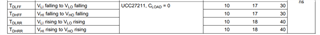
In customer's design, Vin of buck is 80V, Vout is 60V. However, there's 30V pre-bias on Vout when start up. This bias cause the the VHB to VHS differential voltage is below the specified threshold, and UCC27211 enters UVLO. Do you have any suggestions to help start up with this bias for UCC27211?

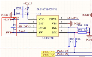
Beside, customer has an idea, which is to add a 12V isolated float power supply between  VHB and VHS. UCC27211 won't enter UVLO with this isolated power. Do you think is there any risk with this method? Thanks.

Regards,

Jiandong 

  • Hello Jiandong,

    Thank you for supporting the UCC27211 with the customer. With the condition you mention, the HB-HS bias will not have a charge path to keep HB charged when LO is not switching. When the PWM pulses start, there would be likely the 1st HO output that may be missed but when LO switches, and switch node transitions to ground the HB capacitor will be charged at that point. If it is possible to have the LO pulse 1st it should help with charging the HB capacitor.

    The floating bias is a solution that can address the concern. The SN6501 is a good solution for the floating high side bias. I would suggest that the VDD of the driver start before or at the same time as the HB bias on the start up sequence.

  • Hi Richard,

    Thanks for your reply. For your first suggestion, as UCC27211 enters UVLO because of the VHB to VHS differential voltage is below the specified threshold, it can't generate 1st LO pulse at all...  For your second suggestion, could you give some more explanations on the start sequence? Will there be any risk when HB bias start before VDD? Thanks.

    Regards,

    Jiandong.

  • Hello Jiandong,

    The UCC27211 LO output will switch as long as the VDD voltage is above the UVLO threshold. If VDD is above UVLO the LO can switch even if the HB-HS bias is below the HB UVLO. The typical start sequence in many cases, starts with VDD over UVLO, HI/LI pwm starts, HB is usually below UVLO until the LO switches and the HS node switches to ground allowing the HB-HS capacitor to charge.

    Regards,

  • Hi Richard,

    Customer find some damage issues about UCC27211 and I describe this issue in attached pdf. Could you please give some suggestions based on attached plots and schematic/layout? Thanks.

    Regards,

    Jiandong

    TP-ZB-60V120A-2B1 V1.1(2021.07.02).PcbDocPower.SchDocUCC27211 damage issue.pdf

  • Hello Jiandong,

    I reviewed the schematic and see a single ~80nC Qg FET on the high side, and a 1uF for the boot strap capacitor. I see that there is a floating bias for the HB supply but for the HB bias to be charged quickly it may be advised to try a smaller bootstrap capacitor value, as long as the HB p-p ripple is low from the bias supply. An HB capacitance of 220nF tp 330nF will be adequate to drive the 80nC Qg with low voltage drop on the HB bias.

    One observation is that there may be Vgs induced spikes during the switching events from the Mosfet drain to gate miller charge. If the Vgs induced voltage is high enough this can cause possible shoot thru. As an experiment, can you try adding some capacitance directly on the Mosfet gate and source which will limit the Vgs voltage perturbations from the miller charge.

    Regards,

  • Hi Herring,

    Thanks for your reply.

    1. Customer used 100nF HB capacitor, but nothing improved.

    2. Customer used 10nF capacitor on MOSFET gate and source, but also nothing improved.

    From the waveforms I attached in last reply, it seems that the drop of high side MOSFET Vgs is caused by SW ring. When customer add a bead on gate or increase the gate resistor, this drop is improved. From layout, the SW area is very large because the large current requirement. Customer believe in that the noise of SW ring coupling to Vgs cause this drop, do you think is it reasonable? And do you think is there any method to prove that this noise is coupling from SW ring? That's perfect if you have any solution besides change the layout. 

    Looking forward to your reply.

    Regards and thanks. 

    Jiandong

  • Hello Jiandong,

    Thank you for the update and additional information about the board layout concerns. I am a little surprised that the capacitance on the MOSFET gate and source did not help. but this is good input that increasing the gate resistance has shown some benefit.

    A large copper area on the switch node results in a larger parasitic capacitance on this node which can couple to ground or other close proximity traces. To avoid board layout change, I think I would try a combination of some things such as somewhat increased gate resistance (or bead) and also the added capacitance on the gate to source. Make sure the HB capacitance can support the added gate to source capacitance. Ex if 10nF is added, increase the HB-HS capacitance by 100nF. Make sure the added capacitance is right on the MOSFET gate and source pins.

    Otherwise, reducing the switch node plane area, and proximity to ground and other traces will reduce the switch node parasitic capacitance and coupling.

    Regards,

  • Hi Richard,

    Thanks for your suggestions. Here are some more questions:

    1. The input voltage is 80V and nominal output current is 60A, do you think how much slew rate of SW rising edge is suitable to this application with your experience? 

    2. Customer use 1pcs UCC27211 to drive 2 parallel MOSFET(Qg=80nC), do you think the 4A peak source current of UCC27211 is sufficient?

    3. To short the gate drive trace of PCB, customer now more prefer to use 2pcs UCC27211(same input for both 2pcs UCC27211) to drive parallel MOSFETs, and still use single L/C filter. I notice that the delay of every units can be very different, the max and min value difference is up to 30ns. I'm afraid that this could cause 2 pcs parallel MOSFET can't turn-on or turn-off at the same time. Do you have some suggestions?  

    4. Based on current situation, do you think is there some better choices than UCC27211, for example, how about isolated drivers? Thanks.

    Regards

    Jiandong.

  • Hello Jiandong,

    With the input voltage of 80V and output current of 60A what I see is a slightly higher than many input voltages which may range from 36V to 75V, but it is not a large increase. The SW node slew rate is normally sufficient since there is 50V/ns rating and if limited to the drivers rating the HS switch time would have to be ~2ns to reach the dV/dt rating.

    For estimating switch time if you assume ~8nF effective capacitance for 80nC at 10V then the Vgs rise time would be Cdv/I. For 4A it would be 20ns if you assume ~1/2 of 4A for average current during transition it would be 40ns. I think this will be OK depending on switching frequency.

     For the idea of using two drivers in parallel, we have not tested half bridge drivers in a parallel driver configuration and there are concerns about driver to driver timing differences especially on the high side floating driver. I would suggest a BJT NPN/PNP buffer for adding more current drive.

    I think there are isolated drivers with higher current drive but I think the higher drive currents are in single channel drivers, so the cost would be noticeably higher.

    Regards,