This thread has been locked.

If you have a related question, please click the "Ask a related question" button in the top right corner. The newly created question will be automatically linked to this question.

LMR33630: based step-down converter burns occasionally

Part Number: LMR33630

Hi,

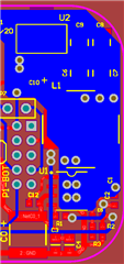
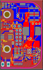
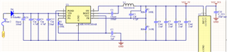
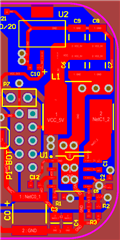
I would highly appreciate your help on the issue we have with step-down converter we designed based on LMR33630CDDAR chip. The design is realized according to TI recommendations including component selection and PCB layout. The schematic and layout are below.

We have developed a device with integrated LMR33630CDDAR based step-down converter. It is supplied from 24V big battery that also supplies other electronics. The whole device is consuming up to 2W, so it should not be overloaded. 95 devices are currently installed at our customer and it is working every day for the last 8 months without any problems, except that in the last few months three of them burned. Once we examined those three we realized that built-in fuse burned. When we shorted the fuse in order to check if it is operational, LMR33630CDDAR burned with lot of smoke and light, like a shiny star.

Can you please check the design shared below and share your opinion what could cause this issue. There is always the option that some external distress caused LMR33630CDDAR to burn out, but I am not sure about that since other electronics would burn too.

Schematic:
Layout Top and Bottom layer (two layers PCB, all components are in top layer): 
          

BOM:

Designator Value Package Manufacture Number
R1, R2 100K; 1% 0603 RC0603FR-07100KL
R3 24K9; 1% 0603

CR0603-FX-2492ELF

C0 100uF; V>=50V; Electrolit   EMZR500ADA101MF80G
C1 0.1uF; X7R; V>=25V 0603 06033C104KAT2A
C2 1uF; X7R; V>=25V 0603 C0603C105K3RACTU
C3, C4 4.7uF; X5R; V>=50V 0805 C2012X5R1H475K125AB
C5 NOT POPULATED 0603  
C6, C7, C8, C9 22uF; X5R; V>=25V 1210 C1210C226K3PACTU
C12 0.22uF; X7R; V>=50V 0603 C1608X7R1H224K080AB
U1 LMR33630CDDAR   LMR33630CDDAR
D4 Schotky; 1.5A; 40V; 0.54V   MBRS1540T3G
F1 50V; 1.5A 1206 044001.5WR
L1 1.5uH; 27A; 2.5mOhm   7443330150

Looking forward to your reply.

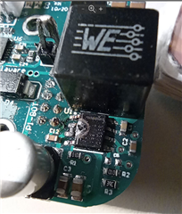
  • Just to add the picture how it looks like once it burns.

  • Hello Ivan,

    Thanks for sharing your schematic, layout, and photo of the damaged device. It sounds like you have seen 3 out of 95 devices become damaged?

    What is your desired output current during normal operation?

    What is the component U2 on the output?

    When you shorted the fuse and observed the device blow up, did you manage to collect any oscilloscope waveforms? 

    Regards,

    Harrison Overturf

  • Hi Harrison,

    Yes, we have 3 damaged out of 95 for the period of 8 months. Just to be clear, all three stopped working without any visible damage because the fuse burned. After the fuse is overridden (shorted) it burns like on the image.

    The normal output operation current is approx. 250mA @ 5V continuous, with short peaks of 400mA @ 5V (every 5 minutes for reading RF card) .

    The 5V output is supplying two 3.3V voltage regulators. one is U2 (LDL1117S33R) and I am not sure what is the other one (I can check if it matters). 

    I did not collect the waveform once it burned.

    Best regards,

    Ivan Petrusevski

  • Hi Ivan,

    Thank you for this information. 

    I suspect that this damage may be caused by an overvoltage event on the input pin when the battery is connected. The ground trace connecting the input capacitors to the GND of the device is not ideal and is adding parasitic inductance that may be adding to any ringing when the battery is connected. 

    Can you try powering up the device with an external power supply rather than with the battery and observe whether the part blows up? I suspect that if you turn on the device with an external power supply you may be able to capture a waveform of the input voltage overshooting. Try turning on the power supply with a lower voltage, 12V and trigger on the rising edge of this input voltage waveform. 

    Regards,

    Harrison Overturf

  • Hi Harrison,

    I can not power those 95pcs. at customer with an external power supply, battery here is the only option here since each device is on a forklift. 

    I did make the oscilloscope measurements of LMR33630 Vin and 5V output using with 12V power supply, 24V power supply, and 24V battery (LiPo, not the same as customer has). The results are in the attached document.

    LMR33630 Vin and VCC_5V.docx 

    Thank you,

    Ivan Petrusevski

  • Hi Ivan,

    Thank you for sending over these images. 

    There does appear to be a significant input voltage spike when the part is turned on. The layout will likely need to be improved in order to minimize this input voltage spike particularly the ground connection from the input capacitors. The EVM for this device can be tested under the same conditions in order to confirm that the layout is contributing to this spike. Please see the layout example provided in the datasheet. 

    Regards,

    Harrison Overturf 

  • Hi Harrison,

    Thank you on your reply.

    The spikes that I saw on input are not that big (violet lines). In case od 24V input, the spike is approx. 15V, incase of 12V input, the spike is 5V. Are those values that significant that can cause the burn?

    I will check the layout in the datasheet, but can you please point on the layout I shared what GND part do you recommend to be changed. I do not have the EVM so I can not confirm those measurements on it. 

    Regards,

    Ivan Petrusevski

  • Hi Ivan,

    I agree that the spikes shown were not large enough to exceed the absolute maximum voltage of the device, however the current required to charge the input and output capacitors are extremely large. 

    Take the output voltage waveform shown in the 24V LiPo battery case. The output voltage spikes up to 6V in ~100ns and the output capacitance is 88uF. Using the equation for capacitor current, i=C(dV/dt) I calculate 5280A of current to charge the capacitors. This could be enough current to violate the Safe Operating Area of the high side MOSFET.

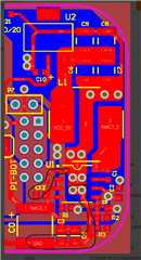
    Below I've circled the GND planes I am talking about. Please compare this with the recommended layout on page 34 of the datasheet.

    Regards,

    Harrison Overturf 

  • Hi Harrison,

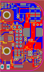
    Thank you for the clear description. We will definitely work on improving the layout and share with you. We have a very limited space here, so we can not follow the datasheet recommendation straightforward.  Can you please check in general if this way would be better? Vin would have to go from top to bottom and to top layer again in this case.

    Solving the GND layout issue should help to prevent burning on power-up. But I am still not sure if it stops working on power-up or during normal operation. I am trying to get this info from the customer. Is there any reason that could cause it to stop working in normal operation, not on power-up? 

    Best regards,

    Ivan Petrusevski

  • Hi Ivan,

    This layout is definitely an improvement with the ceramic capacitors closer to the input pin of the IC, however I suggest using a larger copper pour to connect the SW pin to the inductor. This is the main power path where your load current will be flowing so you don't want to use a tiny trace to connect to the inductor. Have you considered reducing the size of the inductor to save on space?

    If possible, I suggest rotating the R1 resistor 90 degrees clockwise so that you can generate a polygon pour of copper to connect the electrolytic ground pad to the thermal pad of the device. You can still keep the ground trace, but adding the additional polygon help will help ensure a stable ground plane. Alternatively you could place the R1 resistor on the bottom layer and achieve the same thing. 

    At this point I'm not sure what could cause the device to stop working during normal operation. 

    Regards,

    Harrison Overturf 

  • Hi Harrison,

    Thank you on really useful suggestions. Sure the copper pour will be used for the connections, including rotating R1. I have tried a several inductors and had a not so good results. This one was recommended by TI in some document and it works ok, so we did not consider to change it to smaller because it would require a long time of selecting and testing and verifications. If you have some suggestion, please advice.

    Once the new layout boars are produced, I will measure the peaks and get back to you.

  • Hi Ivan,

    I don't have an alternate inductor to recommend at this time. 

    Once your new boards come in we will go from there.

    Regards,

    Harrison Overturf