This thread has been locked.

If you have a related question, please click the "Ask a related question" button in the top right corner. The newly created question will be automatically linked to this question.

LMR36520: LMR36520ADDA, Confirmation for 3.3V and 9V, Audible noise @ -9V

Part Number: LMR36520

Dear *,

we designed in LMR36520ADDA for three different voltage rails 3.3V , 9V, -9V.

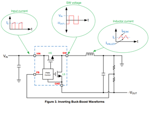
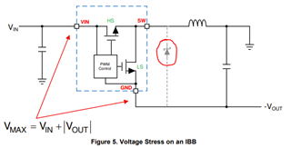
Schematic for all three converters:

3V3_9V_-9V_LMR36520ADDA.pdf

Efficiency measurements for all three converters:

LMR36520ADDA_Efficiency.xlsx

1) 3.3V, please can you confirm that the scope graphs are as expected?

Vin = from 12V to 24V

Vout = 3.3V

Iout_max = 2A

1a) no load switching point  (PFM)

1b) 200mA load switching point (PFM boundary PWM)

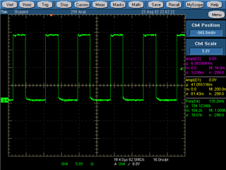
1c) 400mA switching point (PWM)

--------------------------------------------------------------------------------------------

2) 9V, please can you confirm that the scope graphs are as expected?

Vin = from 12V to 24V

Vout = 9V

Iout_max = 1A

2a) no load switching point (PFM)

2b) 140mA load switching point (PFM boundary PWM)

2c) 400mA switching point (PWM)

--------------------------------------------------------------------------------------------


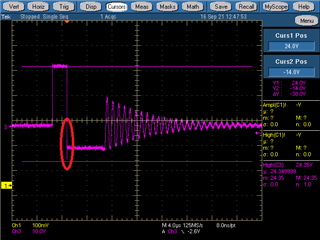
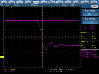
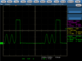
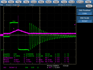
3) -9V, Here we have problems

3a) we hear audible noise when Vin is 12V and the load current exceeds 600mA

3b) we have negative spike when Vin is 24V

Vin = from 12V to 24V

Vout = -9V

Iout_max = 1A

3c) no load switching point Vin 12V (PFM)

3d) no load switching point Vin 24V (PFM) -> negative spike 

3e) 50mA load switching point Vin 12V (PFM)

3f) 40mA load switching point Vin 24V (PFM) -> negative spike

3g) 200mA load switching point Vin 12V (PWM)

3h) 400mA load switching point Vin 24V (PWM) -> negative spike

3i) 700mA load switching point Vin 12V -> audible noise

3j) 500mA load switching point Vin 12V -> transition to audible noise

--------------------------------------------------------------------------------------------

additional information for audible noise 

@ Vin=12 V noise when exceeding 600mA

@ Vin=13 V noise when exceeding 630mA

@ Vin=14 V noise when exceeding 1000mA

--------------------------------------------------------------------------------------------

additional information for negative spiking

when exceeding Vin=19V we start to see negative spiking

--------------------------------------------------------------------------------------------

Best Regards,

David.

  • Hello David,

    In the bottom-most design, you are experiencing some level of  instability.

    Given in IBB design, a RHP zero is introduced into the transfer function, these devices, which internal compensation is geared towards 1/10-1/5 crossover frequency of 400k-2.1M, now requires often a large feedforward capacitor to increase the phase prior to crossover frequency, which I can assume is sub 20k.

    It looks like you have injection resistor placeholder in FB network. Do you have frequency response analyzer available to use?

    I would like to determine actual crossover frequency, then we can see the required CFF to stabilize.

  • Hi Marshall,

    i'm assuming that the comment are about the -9V design ( IBB) and the 3.3V and 9V design are behaving as expected?

    Yes we have in the layout a footprint where we can place a cff. Also there is R287 = 0R ( this is what you mean by injection resistor placeholder?).  We currently don't have a frequency response analyzer available to use.

    Is it possible to determine the crossover frequency with a oscilloscope? If yes, how can this be done?

    What about the negative peak in switching waveform when the Vin = 24V?

    Best Regards,

    David.

  • Hello David,

    yes, my comments are in regard to the IBB. Yes, from the waveforms you shared and the schematics I analyzed for the other designs appear OK.

    It is possible to determine crossover frequency with oscilloscope. "Easiest" way would be apply a load transient which is bandlimited by the control loop. IE: 500mA/uS slew, 1A step (ensure you dont hit current limit).

    Crossover frequency's period is the time it takes for the converter to begin to recover back to nominal set voltage.

    See fig49 

    https://www.ti.com/seclit/ml/slup340/slup340.pdf

    Before worrying about the negative peak on SW, I would first like to ensure we have a stable design. It seems to me we do not at this time.

  • Hi Marshall,

    here are the measurements, please note that we had to set -9V offset on the scope in order catch the transient response.

    If we are measuring correct the f_cross = 22kHz, according to SLVA289B

    Page 5 figure 7.

    Best Regards,

    David.

  • Hello David,

    That measurement makes sense to me and we can see quite clearly you have a stability issue.

    I suggest performing the calculation on required CFF and performing the same measurement to see the delta.

    SLVA834 has a design example in which has similar scenario to what you are seeing.

  • Hi Marshal,

    1)

    we did the calculation per equation 3 on page 4 -> and got 36pF so we used 33pF on the board

    and here are the measurements ( the blue is the load step 1A = 10V / 10Ohm)

    zoomed in

    There is still some oscillation,  also for the noise, last time the noise started ad 600mA load and now it starts at 800mA 

    So there is an improvement. One thing, i was going through my calculation when i designed the schematic and i found out that i designed 

    I_max=0.5A and not 1A ( my mistake), and we have a stable design up to 0.5A and no noise sound. Maybe the noise is because the inductor is not suited for 1A operation?

    2) Newer the less  we have negative voltage spike on sw point when vin = 24V and Iout is below the max 0.5A

    Best Regards,

    David.

  • Hi Marshal,

    i noted one more thing.

    The measurements form my last two post where taken with 1A step and Vin=24V

    Now i changed the Vin to 12V ( because we saw instability under 12V vin)

    Here is a Vin= 12V and 0.5A step and we have fc= 20kHz like before ( no cff)

    And here is a Vin=12V and 1A step and now is the output oscillating and we have fc=10kHz ( no cff)

    Which one should we look at?

    Best Regards,

    David.

  • Hello David,

    I presume, in the instable waveforms, the device is operating in CCM. I am basing that  on that fact you say the issues occurs at lower input voltages, where inductor ripple will be smaller, so inductor zero-cross may not be hit.

    In CCM, for IBB and similar type topologies, a RHP zero is introduced into the system, resulting in some concerns of stability.

    In DCM, the system is single order and inherently stable.

    I would evaluate the CCM waveform. This can be confirmed by measuring inductor current and ensuring inductor current is greater than 0 for a switching cycle, or, the SW node never has a ring on it shortly after low-side is turned on. That ring is a result of low-side turning off, both FETs tristating, and resulting energy sloshing between output inductor and sw node capacitance.

  • Hi Marshall,

    we measured the current through inductor ( we soldered 100mOhm resistor between IC switching pin and inductor).

    1) Vin = 12V, I_load = 0A (no load) , no cff

    2) Vin = 12V, I_load = 100mA  , no cff

    3) Vin = 12V, I_load = 500mA  , no cff

    4) Vin = 12V, I_load = 600mA  , no cff, transition

    5) Vin = 12V, I_load = 650mA  , no cff ( current hits the 0)

    8) Vin = 12V, I_load = 850mA  , no cff ( current hits the 0)

    Best Regards,

    David.

  • Hello David, Plot 8 looks unstable. I would advise going ahead with cff implementation. The design resource I shared give the step by step on the calculation. If you would like for me to review I can.

  • Hi Marshall,

    I'm David's colleague, nice to meet you.

    Unfortunately currently we don't have injection transformer in company but we're planning to get it, anyway we done measurement with step response (470mA Step, V_ in = 12V).

    *Note this converter works in inverting buck mode, V_out is -9V


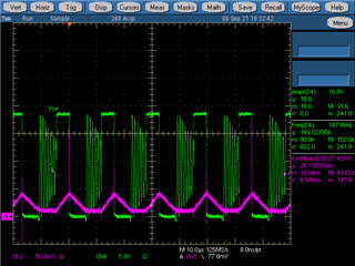
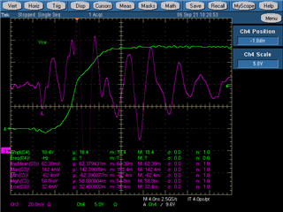
      (Ch1 - V_out transient, Ch2 - Load Voltage transient)

     
    Regarding definition of crossover frequency following Application Report SLVA289B for our case that is 15.62kHz

    otherwise you said before;

    Crossover frequency's period is the time it takes for the converter to begin to recover back to nominal set voltage.


    For Calculation I found a few equations and I'm not sure witch one I need to use

    1) From  LMR36520ADDA Datasheet Cff section say use Application Report SLVA289B


    Solve this equations I got value off Cff ≈ 306pF (R1 = 100k, R2= 12k4)

    2) Application Report SLVA834 equations 

    Solve this equations I got value off Cff ≈ 50pF (R1 = 100k)

    We also tried to blindly put some values of Cff between 15pF and 300pf, but without success. We got even worse cases then without Cff capacitor, the response was with many oscillations or totally unstably system. 

    Regards Mateo

  • Hello Mateo,

    I understand the frustration here. You maybe a little bit light on output cap if CFF is not allowing you to get anywhere stable.

    I would recommend changing ceramic to 4 x 22uF 16VDC.

    Alternatively, you can try adding low ESR electrolytic in addition to the current ceramics ie: 100uF.

    You could do away with CFF by utilizing ESR of electrolytic ie: 50mOhm, but that way can be a bit messy when you consider the tempCo of this ESR.  

  • Hi Marshall,

    Yes you are right about output capacitors, we increased output capacitor from 4x 10uF to 8x 10uF and now we have stable system on output current of  500mA and higher (I checked up to 900mA, and there is system stable)

    1) 24 Vin, 500mA step response


    2) 12 Vin, 500mA step response

    I have another question about negative spike at the switching point, looks image below 

    3)Vin 24V, Without load

    It's that normal behavior? Lower value should be -Vout, he have additional 5V in this spike 

    Maybe we should  use parallel diode like on image below? This image is from Application Report SNVA856A page 6., we didn't find any explanation regarding this parallel diode which impact it has on waveform at the switching point. 


    Regards Mateo

  • Hello Mateo, that is good to hear.

    In regards to negative spike, that seems OK and in the ballpark for what I would expect with a wirebound, hard-switched DC/DC.

    To ensure it is minimized, make sure that you are following layout best practices in the datasheet. If you would like me to review your layout, please open a separate thread for layout review.

    The diode you mention is in regard to a non-sync solution. You are utilizing synchronous control with your converter selection so you need not consider.