This thread has been locked.

If you have a related question, please click the "Ask a related question" button in the top right corner. The newly created question will be automatically linked to this question.

LM7480-Q1: Potential risk with using higher CdVdT

Part Number: LM7480-Q1
Other Parts Discussed in Thread: LM25066, LM74800-Q1

Hi Team,

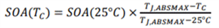
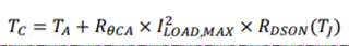
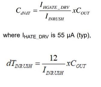
I use datasheet to calculate the CdVdT. The value is around 145nF. But customer only have 470nF in customer factory. Can you let me know if there is any potential risk that we place much higher cap for CdVdT?

Roy 

  • Hi Roy,

    The 470nF cap at gate is very high. This will cause the gate voltage and output voltage to ramp up very slowly. In case there is load current (along with output cap charge current) flowing through the FETs during startup, the FETs may be stressed beyond its SOA limit. 

    The circuit has to be tested during startup, shutdown and all fault conditions. 

  • Hi Praveen,

    So larger cap at gate will cause over SOA potential issue, is it correct? 

    Can you let me know how to select inrush current?

    I follow the datasheet in the beginning, inrush current = 250mA. The calculation result, CdVdt = 145nF. It may be a little large. Our condition is below.

    Cout = 660uF

    Iout = 7A

    Roy

  • FET SOA stress calculation


    A more detailed explanation of SOA calculation is specified in section 2.3 Understanding MOSFET’s Stress Limitations of Robust Hot Swap Design App note.

    For your understanding below is a step by step procedure (extracted from the app note),

    1. Calculate the power stress on the FET during startup. Refer to section ‘2.3.3 Checking SOA for Non-Square Power Pulses’ of the app note.

    Derive t2. Approximation here is  that the FET is stressed for a power loss = P2 = PMAX for t2 duration.

    2. Now, estimate SOA the FET can handle for t2 duration. This value will be at room temperature. Refer to section ‘2.3.2 Checking SOA for Intermediate Time Intervals’ of the app note. 

    Remember that the SOA value in the table below needs to be taken at VDS = VIN(max) in the SOA curve of the FET.

    3. Now, De-rate the SOA calculated in the above step for the Max operating junction/ case temperature of the FET. Refer to section ‘2.3.1 MOSFET SOA Curve and Thermal Model’ of the app note.

    This value can be taken as the temp. of the FET at max load condition,

    4. You can consider that the FET has strong SOA if

    SOA(TC) > 1.2 x (P2 / VDS)

    Where,

    SOA(Tc) is from step 3

    P2 is from step 1

    VDS = VIN(max)

    The factor 1.2 is taken to include a 20% margin.

  • Hi Praveen,

    Thanks for information. But I still have confusion about inrush current parameter. In datasheet, the parameter is 250mA. I have no idea how to define this parameter. May you give me some comments?

    Roy

  • Hi Roy,

    During dvdt based startup, the slew rate of output voltage will be equal to that of gate voltage.

    Igate = Cdvdt * dVgate/dt

    Iinrush = Cout * dVout/dt

    Since, dVgate/dt = dVout/dt

    Igate/ Cdvdt = Iinrush/ Cout 

    Igate = 55uA , Cout, Cdvdt are known. now calculate Iinrush

    Using this Iinrush calculate the stress on the FET and SOA margin. If there is no enough margin, change the Cdvdt and calculate Iinrush and SOA margin once again until the SOA margin is met. 

  • Hi Praveen,

    Thanks for information. Can you help check my design flow?

    Formula.

    Design flow

    1. IHGATE = 55uA, Cout = 660uF(typ), Design IINRUSH is 2A, and we can get CdVdT = 18.15nF(typ) 

    2. Use IINRUSH = 2A to get dT and and also set Vin = 12V, dT = 3.96ms.

    3. Below is MOSFET SOA chart, We use worst case.(right line) VDS = 60V, when current is 2A MOSFET can accept dT> 10ms. 4ms duration is in SOA spec.

    Regards,

    Roy

  • Hi Roy,

    You need to consider the below points while calculations,

    1. The total current flowing through the FET will be = Iinrush + Iload (if there is load during startup). Therefore you need to verify the SOA for Iinrush + Iload
    2. The SOA has to be verified at Vin(max) and not 60V (VDS(max) of the FET)
    3. During startup the power stress on the FET  reduces as the Vout starts raising. This is because the voltage across the FET (Vin-Vout) reduces as Vout starts ramping up to Vin. Follow step 1 and 2  specified in ''FET SOA stress calculation" 
    4. Now the SOA has to be derated for temperature before calculating SOA margin. Follow step 3  specified in ''FET SOA stress calculation" .
  • Hi Praveen,

    Is there any approximate calculation can be referred? I understand you points, but we are hard to get. We are seeking a easy calculation to customer to judge the CdVdT. As my step below. 

    1. For startup, there is no Iload because Vout wasn't built up at that time.

    2. I use VDS(max) because I want to check in worst case.

    I still don't know how to calculate the 3/4 you mentioned above. Can you help calculate it for my reference? our MOSFET https://www.panjit.com.tw/upload/datasheet/PJQ5462A-AU.pdf

    You can assume any parameters in formula.

    Roy

  • Hi Roy,

    For your easy understanding, I have modified the LM25066 Hotswap calculator to suit the LM74800-Q1 startup FET SOA margin calculations. Please find the attachment below. 

    LM74800_Cdvdt.XLSX

    With a Vin(max) = 13.2V , Cout = 660uF and Cdvdt = 22nF, the FET selected has a SOA margin of 3.55. This is a good SOA margin.

    For more understanding on how to use the design calculator, Please refer to the training videos below, 

    https://training.ti.com/node/1133677

    https://training.ti.com/node/1133673

    https://training.ti.com/node/1133664

    You can also deep dive into how each calculation is being made in calculator to understand steps 3-4 in my above message. 

  • Hi Praveen,

    Thanks for information and appreciate your support.

    Roy