This thread has been locked.

If you have a related question, please click the "Ask a related question" button in the top right corner. The newly created question will be automatically linked to this question.

TPS650864: Troubleshooting PMIC used to power Xilinx ZU3

Part Number: TPS650864
Other Parts Discussed in Thread: BOOSTXL-TPS650861, MSP430F5529

Hi,

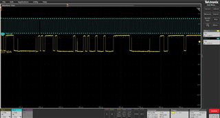
In continuation with my previous debugging query (Before I wanted to bypass BUCK 6 as per your previous recommendation. Also like Bypass means to cut open traces of BUCK6? If we leave BUCK6 unconnected still there will be a Power fault right as i saw in one of the link from IT [FAQ] TPS650864: What to do with unused voltage regulators / rails? - Power management forum - Power management - TI E2E support forums), I wanted to find out and confirm where exactly the Power fault occurred and hence trying to connect I2C BUS to access Power Fault status registers, but i am seeing that the I2C lines on the PMIC are not up and in Idle state the voltage reads as 0.7V to 0.8V. The pull-up resistor is 2.61K ohms and we are trying to connect this bus to an Atmel development board to read the PMIC registers which also pull-up to 3V3.

Following things are provided and working fine with PMIC but not able to identify and resolve the power fault,

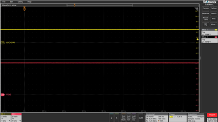
1) VSYS is 12V and is available to PMIC

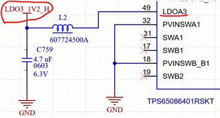
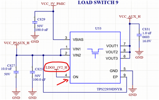
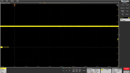
2) LDO3P3/LDO5V0  is available from PMIC

3) Vref 1V3 is available from PMIC

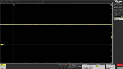
3) CTL1 is provided with LDO3P3

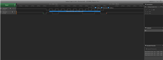
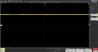
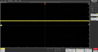
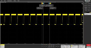
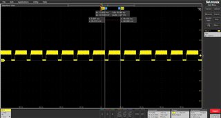
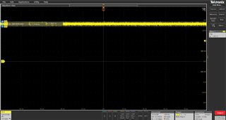
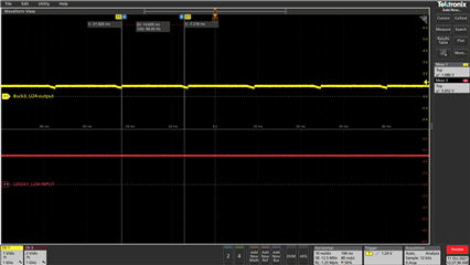
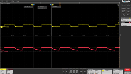
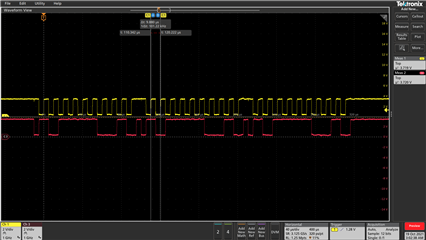
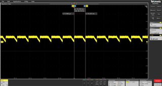
4) Buck1 voltage when reads is at 1V8 but the waveform is as below (Rail, SW, GPO1(+Rail in red))

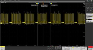
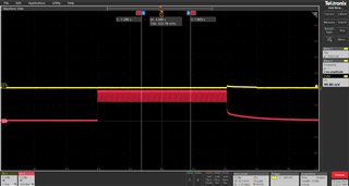
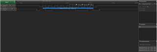
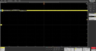
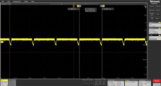
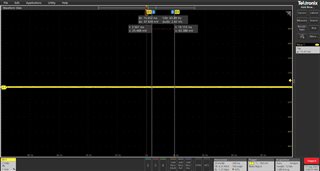
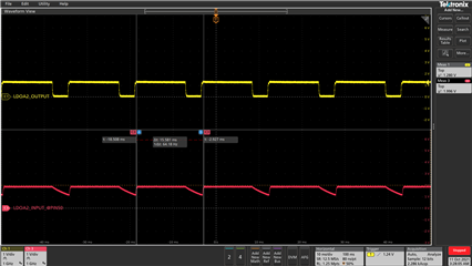
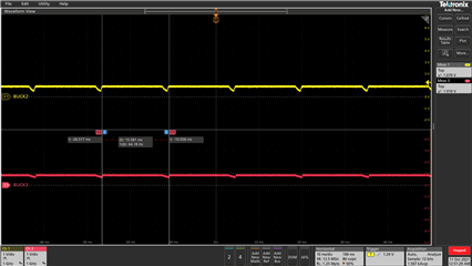
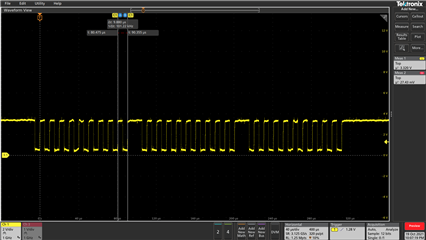
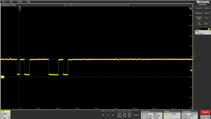
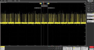
5) Buck2 voltage when reads is at 0V85 but the waveform is as below

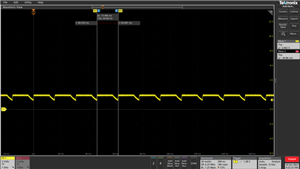
After these 2 Bucks there is no outputs from any of the LDO or BUCKS. 

I am powering up the board for the first time and doing board bring up task. So could you please help in this regard as i am struggling even to see that I2C itself is not working.

Thanks in advance,

Sandeep P

  • HI Sandeep,

    I have assigned the topic to the expert of the device. Due to September 6th being a national holiday in US the response may be delayed. Thank you for your patience.

    Best regards,

    Samuli Piispanen

  • Hi Samuli,

    Thank you for the info. Sure will wait for them to come back.

    Thank you,

    Sandeep.

  • Hi Sandeep,

    Does the I2C work if you keep CTL1 low? IN other words, if the board is powered up but the power sequence is not started are you able to access the I2C?

    Thanks,

    Daniel W

  • Hi Daniel,

    We tried below cases, (Pullup used is 8.66k & 2.61k with Mode set to 100Kbps & 400kbps)

    With CTL1 = High, I2C when read using Logic analyzer is showing NACK.

    With CTL1 = Low, I2C when read using Logic analyzer is showing NACK.

    Please find the waveform of the I2C below,

    100Kbps settings

    400Kbps settings

    Yes the Board is powered up but power sequence is not started and still above is the I2C behavior (There no ACK from PMIC). The address that we are using is 0x5E as per datasheet.

    So please let us know how to proceed.

    Regards,

    Sandeep P

  • Hi Sandeep,

    Can you get a scope shot of the device powering on with VSYS, LDO3P3 and LDO5V0?

    Additionally, can you share a schematic of your design using the TPS650864?

    Thanks,

    Daniel W

  • Hello Daniel,

    Scope shots for,

    1) VSYS

    2) LDO3P3

    3) LDO5P0

    You can find the schematics in this below link,

    /cfs-file/__key/communityserver-discussions-components-files/196/PMIC_5F00_HIGH.pdf

    With Regards,

    Sandeep P

  • Hi Sandeep,

    When is the I2C line voltage at an incorrect level? Does this happen before providing VSYS or after or both?

    Thanks,

    Daniel W

  • Hi Daniel,

    The voltage level issue was resolved as there was a re-work on the board on these I2C lines which was loading the lines. 

    So now we are able to connect the I2C lines with proper voltage pull-up (3V3). But the issue that we are facing now is, when we tried to communicate with PMIC using 0x5E address as per datasheet we are getting NACK and hence not able to read any of the registers specially power fault status registers. We don't know why its not ACK the address. Could you please help to debug this issue?

    Thanks,

    Sandeep P

  • Hi Sandeep, 

    Can you take an analog scope shot of the I2C lines during communication to ensure that they are hitting the appropriate high and low voltages? Additionally, please note that the pmic only supports 7-bit addressing

    Thanks,

    Daniel W

  • Hello Daniel,

    Please find the below waveform form the scope and to our surprise, we were able to get ACK today. Don't know what different we did expect added scope probes to capture analog waveform of I2C. So we are in a process of reading registers to understand the Fault. I will keep you posted once read and then we need to see why PMIC is in Power fault state to resolve it.

    Zoomed version,

    Thank you,

    Sandeep P

  • Hi Sandeep,

    Thank you for the update. Let me know if you get any further insight on this issue or have additional questions.

    Thanks,

    Daniel W

  • Hi Daniel,

    Today we were able to read the registers and then we focused on these below registers data to locate the power fault,

    00h DEVICEID1 Device ID code indicating revision  - 0x01 
    01h DEVICEID2 Device ID code indicating revision  - 0x14
    02h IRQ Interrupt statuses  - 0x88 (FAULT =1 ; SHUTDN = 1; DIETEMP = 0) hence we looked for B0h to B5h registers for root cause.
    03h IRQ_MASK Interrupt masking - 0xFF
    04h PMIC_STAT PMIC temperature indicator - 0x00
    05h SHUTDNSRC Shutdown root cause indicator bits - 0x06  (UVLO =1; PWR_FAULT = 1) hence we looked for B0h to B5h registers for root cause.  (I don't understand why UVLO is asserted as 1, because the VSYS pin is provided with 12V and below is the scope shot for same.)

    B0h PG_STATUS1 Power good statuses for individual rails - 0x0B 
    B1h PG_STATUS2 Power good statuses for individual rails - 0x60
    B2h PWR_FAULT_STATUS1 Power fault statuses for individual rails - 0x82 (LDOA2_PWRFLT = 1 and BUCK2_PWRFLT  = 1)  (For this when we checked on the schematics we are not using LDOA2 and is floating as per TI checklist, and Buck2 is actually showing power fault pattern, attached scope shot.)


    B3h PWR_FAULT_STATUS2 Power fault statuses for individual rails - 0x10 (LDOA1_PWRFLT =1 )

    (when checked on schematics, we are not using LDOA1 and is floating as per TI checklist)


    B4h TEMPCRIT Critical temperature indicators - 0x00 
    B5h TEMPHOT Hot temperature indicators - 0x00

    Also attached the complete excel sheet with all register data captured in it. the observation is when we read multiple times there seems to be a inconsistence in the captured data. don't know why this behavior.  

    I2C_Reg_read data_multi_times.xlsxSendTI.csv  

    So my questions are,

    1) LDOA1 and LDOA2 are not used in our design and are floating as per TI schematic checklist, So why is it still showing power fault?

    2) Since Buck2 is also shown a cause for Power Fault, We are powering up this board for first time and as per datasheet it says "This fields indicates that BUCK2 has lost its regulation".  Can you tell us how can this be possible when we are actually providing inputs to this buck2 and also meeting  the condition of VSYS, LDO3P3/LDO5P0 and CTL1=1 (connected to LDO3P3)?

    Still the PMIC Buck3, Buck4, Buck5 & Buck6, LDOA3 are not up and all GPIO's are showing 0V.

    Not sure how to resolve these power fault issues. Need support.

    Thank you,

    Sandeep P

  • Hi Sandeep,

    I don't understand why UVLO is asserted as 1, because the VSYS pin is provided with 12V and below is the scope shot for same.

    On any POR this will be asserted due to the previous shut-off UVLO and must be cleared.

    For the power fault questions, please include scope shots of LDOA1 and LDOA2. Additionally, I would recommend using the PWR_FAULT_MASKx registers to mask each one of the rails you are seeing faults on one at a time to see if faults persist when the pmic is not continuously restarting. Additionally, if you mask the LDO power faults do you still see one on Buck2?

    For Buck2, an overcurrent could be causing a powerfault if all supplies to the buck are good.

    Please et me know what you find

    Thanks,

    Daniel W

  • Hi Daniel,

    1) So does this mean whenever we do power cycle to PMIC we need to initialize (Read- Check for issues-Write- Read) it to check for any such issues and clear them and then proceed with powering sequence? 

    2) Please find the scope shots for LDOA1 and LDOA2.

    LDOA1:- (not used in design)

    LDOA2:- (not used in design)

    LDOA3 :- (Used in Design)

    We tried something new today. 

    1) since we are not using LDOA1 & LDOA2 and when we saw above pattern, we decided to disable both these LDO's and also cleared there power fault in there respective registers (28h,9Fh and B2h and B3h).  

    2) Once we read these registers and check if it reflected what we want and confirmed, then we just probed Buck1 and Buck2 outputs and to our surprise there were no power fault pattern seen in there waveforms and output voltages were matching with some ripple voltages. This was our first break through in this issue.

    Buck1:-

    Buck2:-

    But unfortunately still Buck3, 4, 5 and 6 are not up yet along with LDOA3.

    Also as soon as we did a power cycle to the board and found all registers are stored with old values and hence the power fault repeated in Buck1 & Buck2. So its not saving the changes that we made to registers. Can you suggest us on how to save these changes permanently into Registers?

    3) Yes tomorrow we will try your point of using PWR_FAULT_MASKx one after the other and see if this will help us to isolate the power fault issue.

    4) I checked the overcurrent reg. B6h and found all were zeros. Hence concluded Buck2 was not affected by overcurrent parameter.

    Need to continue our debugging efforts to find out why other bucks are not up.

    Thanks for your inputs,

    Sandeep P

  • Hi Sandeep,

    Every time the unit is power cycled it will re-load the values from the OTP. However, there are 2 OTP banks on the device so you could program the second OTP bank with these in order to save them permanently. This process is described in the linked document.

    https://www.ti.com/lit/pdf/swcu188

    Thanks,

    Daniel W

  • Hi Daniel,

    Thanks for the OTP link, will use it once we fix the working sequence for all the power rail. 

    By the way the update is I was able to up few of the other rails and below are the list of rails that are up. (Attached are the scope shots )

    1) Buck1 - is up

    2) Buck2  - is up

    3) Buck3  - is up (Forced On using I2C rail enable option)

    4) Buck4 - is up

    5) Buck5 - still not up.

    6) Buck6 - is up (Forced On using I2C rail enable option)

    7) LDOA1 - not used (This is the main reason for causing Power fault as its floating and its PG signal is part of Power good tree for other rails.)

    8) LDOA2 - not used (This is the main reason for causing Power fault as its floating and its PG signal is part of Power good tree for other rails.)

    9) GPO1  - is up

    10) GPO2  -Still not up.

    11) GPO3 -Still not up. (Due to this Buck3 is not turning On, hence did force ON.)

    PMIC_U24_17SEPT2021.zip

    So the summary of PMIC issue was because we didn't use LDOA1 and LDOA2 and due to this there PG outs are part of some the other rails in factory default sequence and hence the power fault. Once these LDO's were disabled using I2C access immediately Power Faults were gone.

    Default Factory sequence:-

    But there are still few issues,

    1) In order to make GPO3 up, we need Buck1,2 &6 PG's, LDOA1,A2 & CTRL1 should be up. But in my case LDOA1,A2 are not used hence using register 0xAB & 0xAA tried to remove LDOA1's PG & LDOA2's PG using LDOA1_msK & LDOA2_msK. But unfortunately after writing these register the LDOA1 & LDOA2 which were disabled using 9F & 28 registers were becoming enabled automatically and PMIC went into Power Fault mode. Can you suggest why this behavior? 

    2) Also for LDOA3 to be up, it needs BUCK3_PG alone and which is available, but still LDOA3 is not up. Hence i tried to force it ON and it went in to Power Fault. can you suggest what could have gone wrong. I need to try disabling the Power fault msk for it and check if its still having the problem.

    3) For Buck6 also I am forcing it to turn ON because it needs BUCK1_PG, LDOA1_PG & LDOA2_PG and there is no option to remove  LDOA1_PG & LDOA2_PG signals from the Power tree for BUCK6. Could you please check this and suggest.

    Thanks for your support.

    Regards,

    Sandeep P

  • Hi Sandeep,

    1) Can you describe the situation the LDOs were becoming re-enabled under? are you disabling before startup and then they are enabling during startup? or after a POR?

    2)  Please ensure that there is no issue with the LDOA3 voltage source when turning it on and that there is not too much current being drawn.

    3)  These are in OTP reserved bits. To change the power trees it is best to use an OTP rewrite.

    In general though, it may be best to return to the root of the issue with all LDOAx showing power faults. can you provide a single scope shot with 2 signals, the supply and output of each LDO?

    Thanks,

    Daniel W

  • Hello Daniel,

    Sorry for the late reply. 

    1) I am disabling them only after POR and in continuation when GPO3 dependents are removed (LDOA1_PG & LDOA2_PG) its re-enabling the LDOA1 & LDOA2. 

    2) I am using LDOA3 output to turn ON the load switch (TPS22959DNYR), so as per datasheet it can be driven with a GPIO pin of microcontroller, so the current requirement is less then 10mAmps to 15mAmps. I did take the scope shot of LDOA3 output pin and its showing zero and no power fault signs in the waveform and input to this is 1V8 on pin 50 (PVINLDOA2_A3)

    LDOA3 output scope shot.

    1V8 on pin 50 (PVINLDOA2_A3) scope shot

    3) I did go though the document that you shared on OTP programming. But in that its mentioned as we need to use two different boards (BOOSTXL-TPS650861 EVM & MSP430F5529 LaunchPad development kit). We don't have them with us and also we cannot remove the PMIC IC from the board to do the OTP programming.

    So my question is, can we use any development board with a I2C capable Microcontroller and interface to I2C bus of PMIC and perform this OTP programming?  (Actually to access the I2C of our PMIC we are using Atmel SAM71 development board and doing all read and write of these I2C registers.) So can we use the same way and do OTP as well? I see that CTRL4 and IRQB pins needs to be supplied with 7V during programming. Also since now the PMIC is in power fault can we still proceed to do OTP programming?

    4) As of now there are no Power Faults except that I am not able to complete the sequence because of LDOA1 & LDOA2 PG's as dependents for GPO3 to come up due to which my LDOA3 and Buck5 are not up.

    Regards,
    Sandeep P

  • Hi Sandeep,

    3) For programming the device, see sections 5 and 6 of the programming guide. The mentioned boards are not necessary.

    1) For the LDOs re-enabling when their PG is removed from a power tree please specify the I2C address and register address and value you are writing when this occurs.

    2) When you say turn on the load switch do you mean that this LDO is connected to a CTLx pin which controls that load switch?

    Thanks,

    Daniel W

  • Hello Daniel,

    3) Yes we tried OTP method after seeing those sections today. But unfortunately it was not successful. the Steps we followed are,

    a) Power ON the board 

    b) Cleared all Power faults using I2C address 0x5E  

    c) Prepared our sequence using OTP excel sheet provide by TI and extracted the raw data from last sheet and used it in our I2C write code.

    d) Provided 7V on CTRL4 and wrote the PROGRAMMING_STATE bit in the OTP_CTRL1 register to 1b

    f) Removed 7V from CTRL4 and provided GND to it. (as soon as we did above step the Power fault occurred again)

    g) we continued the write sequence but we received NACK from there on. Hence couldn't succeed in OTP.

    Please find attached the sequence file extracted from excel sheet.


    PMIC_After_HCL_22SEPT2021_seq.txt
    var custom_program_104 = [		I2C Address (Hex)	Register Address (Hex)	Data (Hex)	Comments
                       {group: 'PART_NUMBER', value: 0x104},		38	02	A0	Can remove 7V from CTL4 after this.
                       {register: 'DEVICEID2', value: 0x11},		38	03	00 or 01	00 for OTP bank 0, 01 for OTP bank 1
                       {register: 'BUCK1CTRL', value: 0x70},		38	5F	00	Sets I2C_Address to 5E (in case it was previously changed)
                       {register: 'BUCK2CTRL', value: 0x5A},		5E	00	04	
                       {register: 'BUCK3DECAY', value: 0x24},		5E	01	11	
                       {register: 'BUCK3VID', value: 0x24},		5E	20	70	
                       {register: 'BUCK3SLPCTRL', value: 0x24},		5E	21	5A	
                       {register: 'BUCK4CTRL', value: 0x3F},		5E	22	24	
                       {register: 'BUCK5CTRL', value: 0x0F},		5E	23	24	
                       {register: 'BUCK6CTRL', value: 0x3D},		5E	24	24	
                       {register: 'LDOA2CTRL', value: 0x0C},		5E	25	3F	
                       {register: 'LDOA3CTRL', value: 0x0D},		5E	26	0F	
                       {register: 'DISCHCTRL1', value: 0x55},		5E	27	3D	
                       {register: 'DISCHCTRL2', value: 0x55},		5E	28	0C	
                       {register: 'DISCHCTRL3', value: 0x15},		5E	29	0D	
                       {register: 'PG_DELAY1', value: 0x01},		5E	40	55	
                       {register: 'BUCK1SLPCTRL', value: 0x70},		5E	41	55	
                       {register: 'BUCK2SLPCTRL', value: 0x5A},		5E	42	15	
                       {register: 'BUCK4VID', value: 0xE8},		5E	43	01	
                       {register: 'BUCK4SLPVID', value: 0x00},		5E	92	70	
                       {register: 'BUCK5VID', value: 0xE8},		5E	93	5A	
                       {register: 'BUCK5SLPVID', value: 0xE8},		5E	94	E8	
                       {register: 'BUCK6VID', value: 0xA0},		5E	95	00	
                       {register: 'BUCK6SLPVID', value: 0x8C},		5E	96	E8	
                       {register: 'LDOA2VID', value: 0xAA},		5E	97	E8	
                       {register: 'LDOA3VID', value: 0xAA},		5E	98	A0	
                       {register: 'BUCK123CTRL', value: 0x27},		5E	99	8C	
                       {register: 'PG_DELAY2', value: 0x00},		5E	9A	AA	
                       {register: 'SWVTT_DIS', value: 0x70},		5E	9B	AA	
                       {register: 'I2C_RAIL_EN1', value: 0x00},		5E	9C	27	
                       {register: 'I2C_RAIL_EN2', value: 0x00},		5E	9D	00	
                       {register: 'PWR_FAULT_MASK1', value: 0x00},		5E	9F	70	
                       {register: 'PWR_FAULT_MASK2', value: 0x28},		5E	A0	00	
                       {register: 'GPO1PG_CTRL1', value: 0xDC},		5E	A1	00	
                       {register: 'GPO1PG_CTRL2', value: 0xEF},		5E	A2	00	
                       {register: 'GPO4PG_CTRL1', value: 0xBF},		5E	A3	28	
                       {register: 'GPO4PG_CTRL2', value: 0xFF},		5E	A4	DC	
                       {register: 'GPO2PG_CTRL1', value: 0xEB},		5E	A5	EF	
                       {register: 'GPO2PG_CTRL2', value: 0xFE},		5E	A6	BF	
                       {register: 'GPO3PG_CTRL1', value: 0xD4},		5E	A7	FF	
                       {register: 'GPO3PG_CTRL2', value: 0xEF},		5E	A8	EB	
                       {register: 'MISCSYSPG', value: 0xFF},		5E	A9	FE	
                       {register: 'VTT_DISCH_CTRL', value: 0x5F},		5E	AA	D4	
                       {register: 'LDOA1_SWB2_CTRL', value: 0x48},		5E	AB	EF	
                       {register: 'BUCK1_CTRL_EN1', value: 0xFE},		5E	AC	FF	
                       {register: 'BUCK1_CTRL_EN2', value: 0xE3},		5E	AD	5F	
                       {register: 'BUCK1_CTRL_EN3', value: 0x09},		5E	AE	48	
                       {register: 'BUCK2_CTRL_EN1', value: 0xFF},		38	07	FE	
                       {register: 'BUCK2_CTRL_EN2', value: 0xC3},		38	08	E3	
                       {register: 'BUCK2_CTRL_EN3', value: 0x10},		38	09	09	
                       {register: 'BUCK3_CTRL_EN1', value: 0xE8},		38	0A	FF	
                       {register: 'BUCK3_CTRL_EN2', value: 0x6F},		38	0B	C3	
                       {register: 'BUCK3_CTRL_EN3', value: 0x10},		38	0C	10	
                       {register: 'BUCK4_CTRL_EN1', value: 0xEC},		38	0D	E8	
                       {register: 'BUCK4_CTRL_EN2', value: 0xE3},		38	0E	6F	
                       {register: 'BUCK4_CTRL_EN3', value: 0x00},		38	0F	10	
                       {register: 'BUCK5_CTRL_EN1', value: 0x7F},		38	10	EC	
                       {register: 'BUCK5_CTRL_EN2', value: 0x6F},		38	11	E3	
                       {register: 'BUCK5_CTRL_EN3', value: 0x01},		38	12	00	
                       {register: 'BUCK6_CTRL_EN1', value: 0xFE},		38	13	7F	
                       {register: 'BUCK6_CTRL_EN2', value: 0xC3},		38	14	6F	
                       {register: 'BUCK6_CTRL_EN3', value: 0x01},		38	15	01	
                       {register: 'SWA1_CTRL_EN1', value: 0xFF},		38	16	FE	
                       {register: 'SWA1_CTRL_EN2', value: 0x6B},		38	17	C3	
                       {register: 'SWA1_CTRL_EN3', value: 0x40},		38	18	01	
                       {register: 'LDOA2_CTRL_EN1', value: 0xFD},		38	19	FF	
                       {register: 'LDOA2_CTRL_EN2', value: 0x43},		38	1A	6B	
                       {register: 'LDOA2_CTRL_EN3', value: 0x09},		38	1B	40	
                       {register: 'LDOA3_CTRL_EN1', value: 0xD8},		38	1C	FD	
                       {register: 'LDOA3_CTRL_EN2', value: 0x8F},		38	1D	43	
                       {register: 'LDOA3_CTRL_EN3', value: 0x89},		38	1E	09	
                       {register: 'SWB1_CTRL_EN1', value: 0xFB},		38	1F	D8	
                       {register: 'SWB1_CTRL_EN2', value: 0xAF},		38	20	8F	
                       {register: 'SWB1_CTRL_EN3', value: 0x09},		38	21	89	
                       {register: 'SWB2_LDOA1_CTRL_EN1', value: 0xFD},		38	22	FB	
                       {register: 'SWB2_LDOA1_CTRL_EN2', value: 0xA3},		38	23	AF	
                       {register: 'SWB2_LDOA1_CTRL_EN3', value: 0x09},		38	24	09	
                       {register: 'OTP_RSVD_38_28', value: 0x18},		38	25	FD	
                       {register: 'SLP_PIN', value: 0x08},		38	26	A3	
                       {register: 'OUTPUT_MODE', value: 0x07},		38	27	09	
                       {register: 'OTP_RSVD_38_2C', value: 0xA1},		38	28	18	
                       {register: 'OTP_RSVD_38_2E', value: 0xAA},		38	29	08	
                       {register: 'OTP_RSVD_38_32', value: 0x61},		38	2A	07	
                       {register: 'OTP_RSVD_38_34', value: 0xAA},		38	2C	A1	
                       {register: 'OTP_RSVD_38_38', value: 0x61},		38	2E	AA	
                       {register: 'OTP_RSVD_38_3A', value: 0xAA},		38	32	61	
                       {register: 'OTP_RSVD_38_44', value: 0x05},		38	34	AA	
                       {register: 'OTP_RSVD_38_48', value: 0x25},		38	38	61	
                       {register: 'OTP_RSVD_38_4C', value: 0x25},		38	3A	AA	
                       {register: 'OTP_RSVD_38_53', value: 0xA8},		38	44	05	
                       {register: 'I2CADDRESS', value: 0x00}];		38	48	25	
    		38	4C	25	
    		38	53	A8	
    		38	5F	00	
    

    Question:- does OTP address 0x38 provides ACK when we remove 7V from CTRL4? Also can we do this OTP even when PMIC is in power fault state?

    1) I2C address used is 0x5E,

           - Register Address is 0xAB (GPO3PG_CTRL2), Data = 0xEF (SWB2_LDOA1_msK bit)

           - Register Address is 0xAA (GPO3PG_CTRL1), Data = 0xDC (LDOA2_msK bit) 

    Also today we saw a strange behavior with GPO3, we have provided 10k ohms of pull-up to 3V3 which i removed for my re-work for OTP purpose as GPO3 is provided as input to CTL4. When I did above register values as I2C write to my surprise there was no re enabling of LDOA1 & LDOA2. I didn't understand this logic of removal of pullup resistor on GPO3 line as its a open drain pin by default. 

    Question:- all other GPOs are have 10K pullup to 1V8 except GPO3. Does this has anything to do with above behavior?  (checked the datasheet for Ele specs and as per that we can provide pullup up to 3V3.)

    2) No. Actually we are using a separate load switch from TI (TPS22959DNYR) and it has an Von pin which is connected with LDOA3 output from PMIC. we are not connecting any CTRLx pin in this path. below is the circuit snapshot.

    Thank you for your support,

    Sandeep P

  • Hi Sandeep,

    It still seems that the main issue here is power faults. In order to better look at the power faults from the pmic, can you supply the pmic with external power sources to ensure that there is no issue with the current on board power supplies.

    For programming, you should be getting ACK from the pmic. A power fault will prevent you from I2C communication if it is causing restarts of the pmic.

    It is odd that removing a pullup changed the behavior. I think scope shots with and without the pull-up would be the best way to continue looking at that issue.

    Thanks,

    Daniel W

  • Hi Daniel,

    1) If its power fault then when we read the I2C registers 0xB2(PWR_FAULT_STATUS1) and 0xB3(PWR_FAULT_STATUS2) it is showing 0x00h as data and also the I2C registers 0x02(IRQ: PMIC Interrupt Register) & 0x05 (PMIC Shut-Down Event Register) are also showing 0x00h values as data.

    Even B0h (PG_STATUS1: 1st Power Good Status Register) is showing 0x3Fh means all the 6 bucks are reaching power good level and B1h (PG_STATUS2: 2nd Power Good Status Register) is showing 0x68h means none of the LDOAx are reaching PG (out of these LDOA1 & A2 are floating and A3 is not coming up even after Buck1, Buck2, Buck3 and Buck6 PG are available as per its PG tree). 

    2) Need to review again. But I2C communication is available even when the PMIC is in Shutdown mode because Vsys, LDO3P3 & CTRL1 is available hence I2C is available as per datasheet reference. 

    3) The behavior remains same that is it read zero volts even if we remove or mounted  the pull-up resistor. No power fault pattern seen. Sorry forgot to get the scope shot for this.

    I had one request, is it possible to have a call  to discuss our issues? So that we can show you live what we are facing.

    Regards,

    Sandeep P

  • Hi Sandeep,

    I believe a meeting will be the best way to communicate current status, goals and next steps. I will email you shortly.

    Thanks,

    Daniel W

  • Hello Daniel,

    As per our yesterdays discussion, please find the scope shots of another PMIC in our design for your review. Even this PMIC is in power fault state as we are not using LDOA1 & LDOA2 But i did observe a difference here and that is LDOA3 is showing power fault waveform (In the other PMIC LDOA3 was showing 0V). 

    PMIC_U29.zip

    I am yet to try the external voltage input for these LDO's .

    Will keep you posted once done.

    Regards,

    Sandeep P

  • Hi Sandeep,

    After discussing with a colleague, It was determined that if an LDO is included in the power sequence it will require a capacitor to avoid power fault.

    Thanks,

    Daniel W

  • Hi Daniel,

    OK, So its almost inline with our discussion on providing a dummy load.

    Sure we will try this and update you on Monday morning. Hope this will also resolve the issues with GPO2 & GPO3. 

    Thanks for your support. Have nice weekend.

    Regards,

    Sandeep P

  • Hi Sandeep,

    Yes this is similar to our discussion about a dummy load, however, no load is required, just a capacitor. And yes, if this resolves the powerfaults I would expect to see the GPOs functioning.

    Thanks,

    Daniel W

  • Hello Daniel,

    Today we tried to add a Cap of 4.7uF/25V 0603 package on Pin #9 (LDOA1) and Pin #51 (LDOA2) bypass it to GND. Well initially there was no change in the output and we were seeing the same old Power faults & PMIC shutdown pattern on scope.

    So next step to debug was to remove the pull-up on GPO3 line and this helped around 50% and we started seeing outputs for Buck1, Buck2, Buck4, Buck6 & GPO1 (This is the first time without I2C programming we are able to see these rails up.)

    But rest of them are still having issue and are not up and those rails are Buck3, Buck5, LDOA3,GPO3 and GPO2 all are showing 0V and there is no power fault or shutdown of PMIC. 

    We are really not able to understand the logic behind GPO3 pull-up causing issue and not sure why LODA3 is never up (even when we did force ON using I2C). I think if we can resolve these 2 issues we may get through rest of them.

    Please suggest if you have any inputs on this behavior.

    Meanwhile tomorrow we are going to repeat adding caps on a different PMIC (U29) and see what is its behavior.

    Regards,

    Sandeep P

  • Hi Sandeep,

    Thank you for the update. Have you tried using an external power supply for the LDOAx supply pins (pin 8 DRV5V_2_A1 and pin 50 LDOA2_A3)?

    Additionally, for LDOA3, I believe you said you had replaced the output inductor in the schematic with a 0Ω resistor. Is this correct? if not please try this if possible.

    for GPO3, please include scope shots of its behavior with and without a pull-up.

    Thanks,

    Daniel W

  • Hi Daniel,

    Today I tried adding the caps for LDOA1 & LDOA2 of PMIC U29 which is a another PMIC on the board. But unfortunately still we see power fault on that as well. 

    Coming back to your recommendation, on providing external power, In order to do that we need to cut the power traces of those pins and then provide a decap. I have requested my manager for doing this change on the PCB and will let you know once done.

    For LDOA3, removed Inductor and provided a 0ohms resistor and still there was no change in the output as is 0V. please find the scope shot.

    For GPO3, I was able to capture scope shot and it is showing as below without pull-up and with pull-up.

    Regards,

    Sandeep P

  • Hi Sandeep,

    Thank you for the information.

    So even though GPO3 never goes high with or without the pull-up, the previously listed resources (Buck1, Buck2, Buck4, Buck6 & GPO1) only turn on when there is no pull-up connected to GPO3.

    This means that without the pull-up there are no power faults from LDOA1/2.

    For GPO3 coming up, without a pull-up there would be no way for this to be up since it is open drain.

    Are you seeing output from VTT LDO?

    Additionally, it looks like the inactive power supplies are triggered by CTL4 which is connected to GPO3 so if it does not come up they will not come up.

    Please try pulling up GPO3 in 2 different ways and let me know the results.

    1. Replace 10kΩ resistor with 100kΩ resistor as recommended in the schematic review guide https://www.ti.com/lit/zip/slva734
    2. If 1 does not work try pulling up to an outside source with a 100kΩ resistor.

    I would try these before replacing the LDO power inputs as the only issue right now seems to be power fault behavior when GPO3 is pulled up and no way to enable CTL4 part of the sequence when GPO3 is not pulled up.

    Thanks,

    Daniel W

  • Hello Daniel,

    Firstly yes VTT LDO is up and available. 

    Yes when there is no pull-up on GPO3 and CTL4 is GND, there are no power fault observed on LDOA1 & A2 and was also able to see the output of 1V8 and 1V2 respectively. 

    Since GPO3 is not up and we had separated it from CTL4, I provided CTL4 with 1V8 from outside source, and the result is started seeing power fault on LDOA1 & A2 as well. when we removed this source and GNDed CTL4 (as we cannot leave it floating as per schematics checklist), the power fault was gone.

    Today we tried the above mentioned point#1(only) and below are my observation,

    We replaced 10K ohms with 100K ohms for the pull-up on GPO3(in-turn connected to CTL4) and GPO2 (in-turn connected to POR of ZU3 FPGA) and to our surprise all the outputs became zero and there was no power fault pattern on any of the power rail.

    We did checked the inputs/outputs of PMIC (VSYS,CTL1, LDO3P3 & LDO5P0) and below are the scope shots. All were good. 

    PMIC_U24_100K_pull-up.zip

    Buck2 SW signal was not as usual and LDOA1 , hence we added there scope shots for your review. Rest all of them were zero volts, hence did not capture them.

    At this point we just got lost and did not knew what was happening with PMIC, and to this even other PMIC which we powered up the day before for the first time is already in power fault even after providing 4.7uF/25v caps on  LDOA1 & LDOA2.

    Please note: Looks like our US Veoneer team is getting in touch with "Matthews, Tyler <t-matthews1@ti.com>" and he may in turn contact you tomorrow to discuss about these issues.

    Regards,

    Sandeep P

  • Hi Sandeep,

    Thank you for the information. We will discuss further tomorrow.

    Thanks,

    Daniel W

  • Hi Sandeep,

    As discussed in our meeting, please investigate the status of the resources following CTL4 (Buck3 LDOA3) through I2C and scope shots. I will continue to look for other suggestions for the GPO3 issue.

    Thanks,

    Daniel W

  • Hi Sandeep,

    I noticed that SWB1/2 are unused but in the power sequence it is stated that they are triggered to come on at 1.8V to create a powergood signal.

    In order to prevent a powerfault from these please add an input source and bypass capacitors to the output.

    Thanks,
    Daniel W

  • Hello Daniel,

    Thanks for your inputs, but there is question need to ask you since we are not using them in our design.

    As per TI schematic checklist,  if we are not using them then we need to connect its source to GND pin and the outputs can be left floating. So we have followed the same. Do you think that this will have any impact on the PG tree of PMIC considering its just a switch and not source for power supply?


    Regards,

    Sandeep P

  • Hi Sandeep,

    In the schematic checklist, "Not Used" means that the resource is not enabled.

    In the TPS65086401 settings in the datasheet, SWB1/2 are used n the power sequence with a PG level of 1.8V and power faults are not masked, so this resource will need to be connected.

    Thanks,

    Daniel W

  • Hello Daniel,

    The surprise part for the day was U24 PMIC which was showing no pulse until Friday evening, suddenly today morning it showed all the outputs. Hence was able to capture below scope shots. 

    As per our discussion in Friday's meeting, please find the scope shots when CTL4 is supplied with 1V8 as in put from external source.

    Case1: Scope shot of LDOA1 Input & Output captured when CTL4 is applied with 1V8.


    Case2: Scope shot of LDOA1 input & Buck3 output captured when CTL4 is applied with 1V8.

    Case3: Scope shot of LDOA2 Input & Output captured when CTL4 is applied with 1V8.(Note: In this case we are seeing power fault pattern in Input  for LDOA2 because that supply of 1V8 is provided from Buck1 of same PMIC U24)

    Case4: Scope shots of power fault observed on other power rails when CTL4 is applied with 1V8.

    With Regards,

    Sandeep P

  • Hi Daniel,

    OK Let me work on this and provide you an update.

    Also I would like to let you know that we tried today to provide I2C access to another PMIC on board which is already showing power faults on all the power rails even after providing caps on LDOA1 & LDOA2. But the strange thing we observed is even I2C lines are showing power fault patterns instead of steady 3V3 since its pulled up . Need to do more debug on it as well. will share scope shots tomorrow.

    Regards,

    Sandeep P

  • Hi Daniel,

    Regarding your previous reply on providing source for SWB1/2 and de-caps on there outputs. My thoughts after reviewing the OTP excel sheet matrix (which represents the default datasheet values) is even if we bring up SWB1/2 PG signal it contributes to only GPO2 output and still GPO2 will not come up because it also require LDOA3 output which is showing 0Vs from day one. And for LDOA3 to be up we need Buck3 PG to be up and its not possible until we resolve CTL4 causing Power fault when provided with 1V8 or 3V3 as input.

     Regards,

    Sandeep P

  • Hi Sandeep,

    You are correct. However, I think it is relevant to be prepared to continue the power sequence with each resource.

    In regards to the issue appearing between CTL4 and LDOA3, the most likely issue is Buck2. Is Buck2 currently loaded, and if so would it be possible to remove this load?

    Thanks,

    Daniel W

  • Hi Daniel,

    Yes currently Buck2 is loaded, it is connected to PSINTFP & PSINTLP which is having a low resistance path of 5ohms to 10ohms range.

    I tried removing the load, and did check the outputs of Buck4 & Buck5 but its still showing 0V. Hence no change in behavior.  Below is the scope shot from Buck1 after we provided CTL4 with external 1V8. we see power fault getting introduced.

    second point/issue : regarding the other PMIC (U29), we tried to tap the I2C and read the PMIC registers, but we are getting NACK. Below is the snap shot of the SCL & DATA lines of I2C. we have configured it for standard mode & pull-up used are 8.25K ohms to 3V3 rail. Not sure why PMIC is sending NACK.

    I Have checked the VSYS=12V, LDO3P3 and LDO5P0 are available.

    The idea of bringing this PMIC through I2C approach is to make sure we can access the Med FPGA and then we can give the board to software team so that they can work on firmware development related to Automotive Ethernet and this feature of the board is available only for Med FPGA & MED PMIC. 

    So that software team can make good progress in firmware development and we can parallelly work with you on the board that Le Laplant would share.  

    But due to this NACK issue not able to get access for Med PMIC to remove the power faults and proceed with programming/flashing Med FPGA.

    Regards,

    Sandeep P

  • Hi Sandeep,

    The absolute maximum rating for the I2C pins is 3.6V but it appears in the scope shot that the line goes to 3.7V. Please adjust the voltage accordingly to not exceed the absolute max rating. After doing this, let me know if the issue persists

    Thanks,

    Daniel W

  • Hi Daniel,

    The scope shot setting is set to Top , so while doing single shot capture with trigger we could see the top voltage level as reading but it is just a spike of noise and not the actual level of the signal.

    To clear this we took scope shot of I2C-SCL & I2C-SDA separately and you can see that its within the limit of 3.6V as per datasheet. Also captured the Saleae tool data logger to show the NACK.

    1) I2C-SCL


    2) I2C-SDA

    3) Saleae tool data logger output.

    With Regards,

    Sandeep P

  • Hello Daniel,

    Further to above reply, since we couldn't get access through I2C. We started debugging to find out what is causing power fault and in this direction we just removed the outputs from BUCK1, BUCK2  & BUCK3 and then checked for the power fault. BUCK4,5 & 6 are showing 0V. 

    But Buck1,2 & 3 are still showing power fault pattern (scope shots were shared in above reply chain). at this point we checked inputs/outputs VSYS, LDO3P3, LDO5P0 & CTL1 and all were good. below is the scope shots for same.

    Not sure what else is to be debugged for power faults location. 

    Regards,
    Sandeep P

  • Hi Sandeep,

    Thank you so much for clarifying on the I2C levels. So from my understanding, This pmic is behaving similarly to the other one but without I2C access. I would recommend going back to the first pmic and trying to enable each rail individually using the I2C_RAIL_ENx registers and seeing if any power faults occur when rails are on individually?

    Thanks,

    Daniel W

  • Hello Daniel,

    This pmic is behaving similarly to the other one but without I2C access.

    No, This PMIC is not behaving same as the first one. below are the reasons,

    1) when CTL1 is connected to GND instead of LDO3P3, still we can see power fault pattern in BUCK1,2,3 & LDOA1, Buck4,5,6 & VTT LDO all are at 0V even when CTL1 is at LDO3P3. (But in case of 1st PMIC with I2C access, when you connect CTL1 to GND all the outputs will become zero, hence matches with datasheet definition.)

    2) We provided those 4.7uF/10V caps on LDOA1 & LDOA2 but still we are seeing power fault pattern. (But in case of 1st PMIC with I2C access, as soon as we provided de-caps those LDOA1 & LDOA2 started showing there respective power rails clean 1V8 & 1V2.)

    3) The changes that we did to access I2C on this PMIC is same as 1st PMIC, but we are getting continuous NACK.(But in case of 1st PMIC we did get the access to I2C and were able to read & write to reset Power Faults and many other things with all I2C registers)

    I would recommend going back to the first pmic and trying to enable each rail individually using the I2C_RAIL_ENx registers and seeing if any power faults occur when rails are on individually?

    Yes we have already done this and successful flashed FPGA after completing the Power sequence manually using I2C approach. below are the steps we did, Read the I2C register and clear the power faults and then below things happen 

    1) Buck1 - is up

    2) Buck2  - is up

    3) Buck3  - is up (Forced On using I2C rail enable option)

    4) Buck4 - is up

    5) Buck5 -  is up (Forced On using I2C rail enable option)

    6) Buck6 - is up (Forced On using I2C rail enable option)

    7) VTT LDO - is up

    8) LDOA1 - not used (Hence disabled using I2C approach)

    9) LDOA2 - not used (Hence disabled  using I2C approach)

    10) GPO1  - is up

    11) GPO2 -not up.

    12) GPO3 -not up. (Due to this Buck3 is not turning On, hence did force ON.)

    13) CTL1 is provided with 3P3 

    14) CTL4 is presently GNDed , if connected to 1V8 or 3V3 will introduce Power Fault to the system

    15) CTL2,5 is GNDed

    16) CTL6 is connected to GPO1 hence its functional.

    There were no power fault after you do I2C approach on any of the rail and that is why we wanted to know how can we make PMIC standalone to work as per our power sequence. 

    To summarize, There are no power faults that stays once you clear them using I2C approach and hence some of the power rails are up by themselves and some are not hence need to do force turn ON, which means they are bypassing the PG tree and hence turning ON. 

    So I am feeling that something is gone bad with GPO's and CTL's PG tree logic, which is why we are seeing these power faults, because as soon as you remove dependences related to these, all the BUCK's will work fine (This is not true in the case of 2nd PMIC). 

    In our board we have total of 3 PMIC's out which I have explored 2 of them, from tomorrow I will explore 3rd one to see how it behaves compared with other two.

    With Regards,

    Sandeep P

  • Hi Sandeep,

    Thank you for the detailed summary on the differences. Please keep me updated on the behavior of the third pmic. I will continue to review this case. Please expect an update by tuesday on my end.

    Thanks,

    Daniel W

  • Hello Daniel,

    Today we verified the 3rd PMIC and unfortunately even this PMIC has power faults. All the Inputs to the PMIC are available and good , but we could see power fault pattern in Buck1, Buck2,  Buck4 LDOA1 & LDOA2. But Buck3, Buck5, Buck6 and LDOA3 are all at 0V. 

    We even provided the de-cap of 1uF for LDOA1 but still power fault was present, below is the scope shots of the power faults rails& inputs to PMIC only because rest of them are at 0V.

    3rd PMIC U21.zip

    But one positive note that we observed here is, if we GND CTL1 pin then those power fault rails are going to 0V level. So we are assuming it may behave similar to 1st PMIC (U24). So we will have to debug further on CTL4 line behavior to see if that is source of power faults. 

    With regards,

    Sandeep P

  • Hi Sandeep,

    Thank you for the update. I will look into more debug solutions and update this thread by end of day tuesday.

    Thanks,

    Daniel W