A related question is a question created from another question. When the related question is created, it will be automatically linked to the original question.
If you have a related question, please click the "Ask a related question" button in the top right corner. The newly created question will be automatically linked to this question.
Could you please provide a description of the issue they are seeing?
I don't fully understand the document attached. Would it be possible to provide a version translated to English?
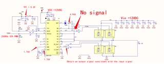
If I understand correctly, their switching frequency is 200kHz (50% duty cycle), Vin = 12V. What's their Vbus voltage?
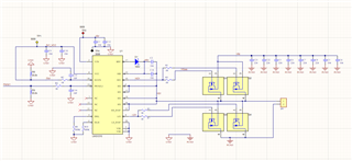
From their schematic, seems like they are using 100nF cap for the bootstrap capacitor and the VDD capacitor. We recommend the VDD capacitor to be at least 10 times larger than the bootstrap capacitor. Can you please ask them to increase one of the VDD capacitors? They already have 1nF, they can change the other VDD cap for a 10uF cap.
Thank you for the information. Could you please remove the resistive load on the switch node (30 Ohm resistor) and see if the issue is still present when the load is removed? It would be best to test this on a new board.
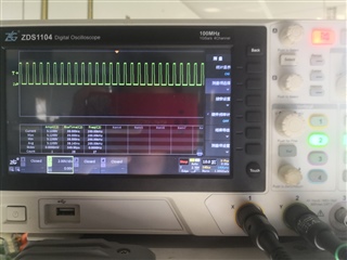
If issue is still present, please, still with the load removed, capture on a single oscilloscope plot: VDD, EN, PWM, LO. And in another oscilloscope plot: PWM-VSS, HB-HS, HO-HS, LO-Vss (you'll need to use differential probes to measure HB and HO with respect to HS). Please measure all signals as close to the pin as possible and using tip and barrel method. The reason for having the signals requested on a single plot is to be able to see the timing between the signals.
Thank you for your reply. We have tried to remove the 30 ohm test resistor. When the test condition is EN=5V PWM=20Khz~1MHz, most of the board's HO pin has no signal, and some of the board's HO pin remains high and large. The LO pins of some boards can be tested to normal PWM signals.
I want to confirm the steps that I need to do. Step 1. I need to use an oscilloscope to test the waveforms of VDD, EN, PWM, and LO. Is this relative to VSS? . Step 2. Test PWM-VSS, HB-HS, HO-HS, LO-Vss. My current equipment is a four-channel oscilloscope, but I don’t have a differential probe. Can there be other ways to confirm the signals of HB-HS and HO-HS?
Thank you for your help and look forward for your reply
Question about step 1: Yes all these signals with respect to Vss.
Question about step 2: In that case you can take these 2 plots below:
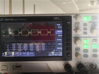
One plot with PWM-Vss, HB-Vss, HO-Vss, HS-Vss (and with the oscilloscope use the math function to subtract HB - HS signals)
2nd plot with PWM-Vss, HO-Vss, HS-Vss, LO-Vss (and with the oscilloscope use the math function to subtract HO-HS signals)
When you capture these please capture one where we can see a few cycle, and other plot with a smaller time scale where we can see 1 or 2 full cycle with higher resolution.
Thank you for providing the plots. I'll analyze them with our team to give you feedback by tomorrow.
Does this issue happen during startup? Does HO signal eventually starts switching?
The reason I ask is because there is a startup delay that you need to take into account before you start switching the low side and the high side. The optimal startup sequence is to rise VDD voltage level about UVLO and then wait tSTLS (150us) before switching the low side. Similarly, once HB-HS voltage level is above UVLO, then you should wait tSTHS (28us) before switching the high side.
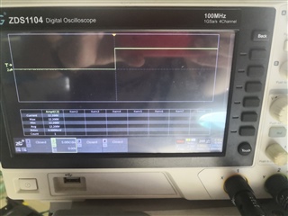
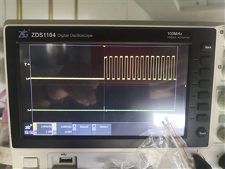
I could only got a waveform at the HO pin at the moment of power-on.
2、Does HO signal eventually starts switching?
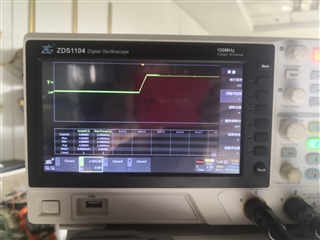
Except for the moment of power-on, the HO pin is always low during the rest of the time, but the LO pin is always a normal PWM output。
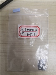
I have 40 PCS LMG1210 chips now,But most of the circuit boards are like this.
I am thinking that the quality of the chip I obtained may be defective,But TI’s official website is not available, and other authorized agents are also not available.
So I asked the team for help to analyze if my application was improper.
Thanks for providing the waveforms. It seems like HB to HS voltage level is staying at ~0V. I think it would be best to test the driver by itself to make sure it is working correctly.
To understand if the driver is working correctly, you can turn off the Vbus voltage (VIN on your schematic) and remove the load and test this way, and monitor HB to HS, HO to HS and HS to VSS.
If you are still seeing the same behavior, you can then check the basic functionality of the driver without any load, Vbus or FETs. In this case, you would remove the FETs (you can do this by removing the gate resistors) and short HS to GND. This way, you should be able to see both high side and low side signals switching (both with respect to GND).
We have confirmed that HB-VSS HO-VSS is always 0 after many times, except for the moment of power-on.Almost all boards can output normally on the LO pin.
I just followed your suggestion by removing the drive resistance and turning off Vbus, but the situation remains unchanged.
Leslie is out of the office at the moment. It appears you have an extended conversation going, she should be available tomorrow to address the recent questions.
Thanks for the information. Just to confirm, when you did this latest experiment, did you short HS to GND?
I think it is unlikely that these are defective ICs (specially since you are seeing several of them showing the same behavior) since all the devices get tested in production. I sent you a friendship request to be able to discuss in private messaging further debugging steps in more detail.
Glad to receive your reply so quickly,I can confirm that HS is shorted to GND.
As you said “I think it is unlikely that these are defective ICs (specially since you are seeing several of them showing the same behavior) since all the devices get tested in production”
the almost all boards have the same phenomenon, I also don’t think all chips have problems.But there is a situation I need to explain, my chip is not directly purchased from TI, because the official website is out of stock,I bought the chip from Shenzhen Huaqiangbei Trading Market,
Thank you very much for sending me a friendship request, but where should I see this information? I’m very sorry, I’m not very clear about to use this platform
In the very top corner on the page you should be able to see a message box when you're logged in. This will take you to your massages page where you can keep communicating with Leslie.
Leslie is out this week and I will be helping you.
-------
With these devices being purchased from the Shenzhen Huaqiangbei Trading Market (SEG Plaza?), I know there are many devices being sold here, many of which can be fake. I will check internally if there is a way to check the authenticity of the devices.
In the mean time, could you please help with the following?:
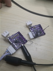
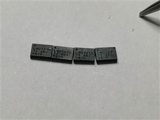
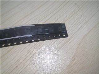
1) Provide a close-up picture of the devices so that I can read the numbers on the chips?
2) Provide a picture of any documentation that came with the devices.
3) Check to see if there are any short circuits on the board from HO to HS and HO to GND
-------
Like you said, if possible, it is always best to purchase devices directly from TI.com
Regarding my question, I was wondering if you could send a picture of the box or bag that the devices came in (with any labels, etc). No worries if you cannot find it.
Thanks for the close up photo of the parts! I will check with our internal team to see what conclusions we can come to.
-------
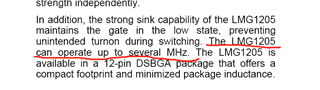
Regarding the maximum frequency of the LMG1205, we do not specify it because it will depend on how much capacitance it must drive on the gate of a transistor, along with the resistance in the output path of the driver. This dependency comes from how much heat the device will create at these fast switching speeds and if it can dissipate the heat (along with allowable rise and fall times). This will depend on the thermal resistance specifications in the datasheet, the PCB, ambient temperatures, and load it must drive.
-------
Another thing we can try in your current set-up is removing one of the bootstrap capacitors, as two 0.47uF caps may be too much. Please let me know how this goes.
I got chips from two suppliers,One is packaged and the other is in bulk
Reply to your question about the bootstrap capacitors,0.47uf is the parameter in the demo board,We had tried to use 0.1uf, 2.2uf,the result is the same HO is always no signal,LO is always normal output
Thanks for your reply,As I reported, almost all the HO chips have no output,We had tried to remove the drive resistance test chip according to Leslie’s suggestion.
I have two circuit boards, all parameters are exactly the same, it can work normally, the waveform is also normal, only 2
At present, I can’t find any other possibilities, maybe the only possibility is that the chip I got should be abnormal
Thank you very much for your help,
From the performance point of view, LMG1210 is a very good choice for my product. Unfortunately, I cannot order it.
I am going to use LMG1205 to design a high-frequency half-bridge driver, because I can order this chip from TI.
My name is Jim Davenport and I am the TI Anti-counterfeit Program Manager. I am sorry to inform you that Shenzhen Huaqiangbei Trading Market is not a TI authorized distributor. Due to uncertainties in the supply chain regarding chain of custody of the products, TI will only support product verification requests from customers who purchase through authorized distributors. All other verification requests must be worked through their supply chain.
I found out www.mouser.com today that there are LMG1210 chips on sale. I have already purchased some samples. I will try again when the chips arrive. If the situation is still the same, I will consult again.