This thread has been locked.
If you have a related question, please click the "Ask a related question" button in the top right corner. The newly created question will be automatically linked to this question.
Hello
I am hoping someone who has experience with UCC256404 or TI mastermind could help me with the design.
Design Parameters:
DC voltage range: 260 315(nominal) 340 VDC
AC voltage range: 185 ~240 VAC
VOUT Output voltage - Normal mode Burst mode threshold to full load = 25 A 24 VDC
I am designing a UCC256404 based LLC Power supply for 24v 600watts at full load. I am not using the PFC boost UCC28070 for now and using a bridge rectifier and RC filter to get Dc nominal voltage at Vin .i am trying to get the UCC256404 to work but I am having a problem starting up the IC. Since I am not using the PFC boost correction phase so I have set the DC bulk voltage between 260V DC -340V DC at nominal DC input voltage as 315V.(220VAC~50Hz Mains).
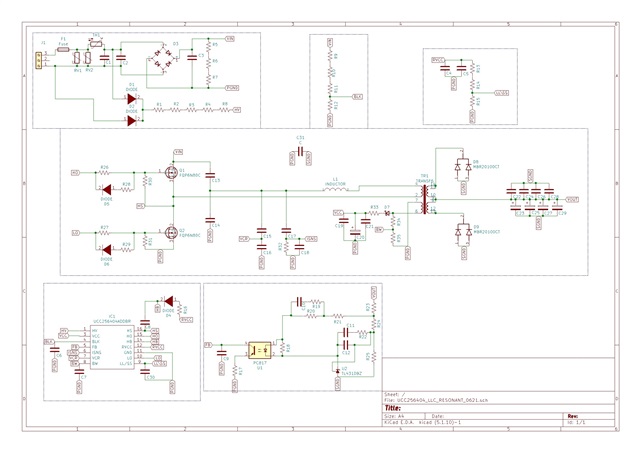
I have calculated the values using the UCC25640x Excel sheet Calculator. Please find it attached below. I have connected a 24V DC Motor which works at 48Watts at the load. The resultant switching frequency(resonant) is ~98kHz.I have attached the schematic and BOM for reference. Can you please check and what could be the possible error for fault. From what I have analysed through the waveforms, I would like to make few points for you to review-:
1)Vcc turns and goes till 26 Volt and then settles down to 14.3V as calculated nominal bias winding but the RVcc pin jumps to 13.5V Mean(when Vcc is around 26V)and then goes low when Vcc settles to 14.3V.This is irregular with what is expected from RVcc as Rvcc needs to be constant at 13V when Vcc starts switching.(Reference:UCC25640EVM-020 Evaluation Module ,Literature Number: SLUUBX3B Fig7) .
Also I don't understand that why the Vcc voltage stays constant at 14.4 volt as the mosfets are not switching in steady state as discussed in point 3.Is it because the Elco capacitor connected to Vcc gets charged but I don't see it discharging even remotely. It seems to be constant voltage coming from the 3 number pin of the IC. Shouldn't it be other way around that the pin3 is the input pin and not the output.
2) The HB-HS pin starts with a pulse but eventually the signal dies after few ms.The HB-HS<17V is satisfied during those milliseconds. The following waveform appears-
Blue-HB Yellow-HS
I am also a little unsure of how HS-HB works. HS works as the ground for when high side gate drive current,right?This means it acts as ground when high side mosfet is on?
and HB acts as the high side gate driver floating voltage charged from Rvcc when the lower mosfet is on. What I don't understand is why the high side mosfet would need a floating voltage when it is turned off(ie when low side mosfet is conducting). The high side gate voltage should be not positive at that time as both the mosfets work as compliments to ensure zvs and llc resonant working condition.
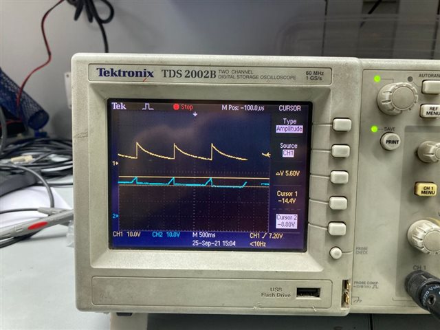
3)I am not getting a startup LO pulse but rather an abrupt burst of HO and LO pulse. Please refer to the diagram below.
Blue-LO Yellow-HO
When the 24V 2Amp load is connected , and input AC voltage is at ~185VAC(~264VDC calculated Bulk startup voltage), the IC seems to restarts every second for the maximum number of counts(5-6) but when the input AC Volt is increased to 220VAC(315VDC-Nominal Vin), the IC stops with reducing number of restart counts.The rotor on the motor makes progressive minimum angle rotation at each restarting pulse from the IC.
4) The BLK pin seems to be working fine with Mean DC voltage at BLK pin =1.2V (Rblk lower=38kOhm Rblk upper=10MOhm and Cblk=10pF).
I have attached the zip file including the schematic,BOM, excel sheet calculator with my specs and the transformer specs.
Please help me debug the issue and let me know what I am missing.
Thanks in advance.
Hi Rahul,
First of all, I couldn't access the attached zip files.
As you can see in the above picture, format of the attached files got corrupted.
After reading your comments, I thought following Inputs will help you for debugging:
1. You can see the Bootstrap working principle in the following link:
Bootstrap Circuitry Selection for Half Bridge Configurations
2. When you measure HO with respect to HS, you should use differential probe. If you use single ended probe, HS will always be connected to ground through the oscilloscope. So, the converter doesn't work.
3. Design of the converter is done for 600Watts. However, when you operate at 48W,converter might operate in burst mode. During this mode, converter switches for some time and then both switches will be off for some time. So you should expect burst packets during this mode (see the burst mode control section in the UCC256404 datasheet). You would see these burst packets only when there is a sufficient RVCC voltage. If there is no enough voltage on the RVCC pin, due to under voltage lock out (UVLO) protection, you wont see any pulses. When a fault occurs (in this case might be UVLO), RVCC will be zero. You can see this in the below picture. If the IC is in fault condition, It will stop operating and will restart after 1sec.
4. During burst off period, since both the switches are off, there is no energy from the bias winding to the VCC pin. Energy needed to turn on the upper mosfet after bust off period will be provided by boot strap capacitor. So, you need to make sure you have sufficient voltage on the boot strap capacitor soon after you come out of burst off period. To design the Boot strap capacitor see power supply recommendations in the UCC256404 data sheet.
5. Just for debugging purpose, you can operate the converter at the higher load. That way you wont be operating in burst mode. Observe the LO, HO waveforms, VCC and RVCC waveforms. Make sure you are using right probes and high band width oscilloscope.
6. For more details about VCC and RVCC, please go through page 42 and page 45 of the UCC256404 data sheet. If you still have questions about these VCC and RVCC pins, feel free to reach out.
I hope these comments helps. Let me know if you have further questions.
Regards
Manikanta P
Hey Manikanta
Thanks for the quick reply. I have attached the schematic(pdf and Jpeg) and the BOM of my design again as you mentioned the previous zip files got corrupted. Please let me know if you can access these files now.
Thanks for making all the points, they were pretty informative. I have a few things I would like to discuss as referring to the points you made as follows-
1)I have gone through the link you shared and calculated the values as following-
Cboot>1.1nF
Cboot=2.2uF(selected value)
Rboot=75Ohm(Length of charge boot state=300usec-reference ucc256404 pg9)
Cvdd>22uF
Cvdd=20uF(selected value)
These calculations were made referenced to slua887( eq2, eq5, and eq6).
I was using general purpose diode as Dboot,I changed it to SS54(schotkky diode). and Rboot =75Ohm. Also I added the Rbias and Cvdd as follows-
Cvdd= 20uF Rbias= 220Ohm
(I have assumed Rbias to be 220Ohm, Let me know if this assumption is correct and how to calculate Rbias).
I think I have made some progress as the IC is restarting every 1 second now .
These are the HO LO wavepulse .
2)I have measured the HO & LO pulses with respect to the ground using a single-ended probe. Is that an issue? For measuring HO wrt HS, I will use a differential probe. As you mentioned the converter will not work when the single probe is used for measuring HO wrt HS, can I use a single-ended probe to measure HS and HB wrt IC ground? I have attached the results in the main post after point 2. I currently don't have the differential probe and have ordered it.
3) Also I can see the RVCC and VCC continuously varying, I think as you mentioned it is going into UVLO but what should be done regarding that? Can you please guide me.I have varied the input voltage from 180VAC~240VAC and it looks like IC stops switching below 180VAC and restarts only after 180VAC.
These are the RVCC and VCC voltages I am getting on the CRO.
4) As for the voltage across Cboot Capacitor, I am measuring using the single ended probe. The Cboot voltage is mean ~3V.
Yellow-Cboot Blue-LO.
5) I am using a 5 ampere load for now and arranging for higher load. I am trying to make the 5 ampere load but there is no progress. The open voltage is coming out to be 1.5V. Shouldn't that be 24V even if there is no load at the output?
Your comments were really helpful. I hope the circuit needs a little tuning to make it work. Hope I can figure it out with your help.
BOM_final_pdf.pdfTransformer 24V-25A _final_pdf.pdf
Please find the attached BOM and Transformer specs for the reference.
Hi Rahul,
I am glad that the links that I shared were useful.
You can refer following 1kW LLC reference design. Since it's close to your power requirement (600W), this should be really helpful.
TIDA-010081 reference design | TI.com
1. For bootstrap design please refer page number 67 in the datasheet UCC25640x LLC Resonant Controller with Ultra-Low Audible Noise and Standby Power datasheet (Rev. E) (ti.com). Also you can compare the obtained results with the 1kW reference design and EVM design (UCC25640EVM-020 User Guide (Rev. B) (ti.com)). Rboot in both of the reference designs are around 2ohms. So, I would recommend changing Rboot value to a lower value.
2. There should not be any Rbias resistor for charging Cboot. Only Rboot is sufficient. Please refer EVM and 1kw reference design schematics.
3. Its better to measure all the signals with the differential probes just to be safe. When HO signal is measured with respect to ground, I would expect the voltage to be vary between Vin+Vboot to zero. But I don't see this happening in the oscilloscope waveforms.
4. cboot voltage should not measured with single ended probe. If you do, switching node will be shorted to ground through oscilloscope gnd through probe gnd. So, the converter does not work. (Can you make sure the mosfet devices and controller are not damaged)
5. Since there is no enough voltage on the Cboot, controller is going to the fault mode where controller will keep restart after 1sec. The controller should not be in this state as it will cause overheat to the controller and it might get damaged.
6. The converter is in fault mode. So, I wouldn't expect output voltage to be at 24V.
6. So, make sure you are getting expected voltages on the VCC and RVCC pins. These voltages needs to be constant. Otherwise there wont be any switching. Also make sure you operate the converter at the higher load just for debugging purpose.
Let me know if you have any further questions.
Regards
Manikanta P
Hello Manikanta,
Thanks for the quick response.
I would like to update you on the circuit changes I made based on the references you provided. Also, the mosfets and controller are fine.
1) Removed Rbias and changed Rboot to a lower value=2Ohm(75Ohm earlier).
2) Increased the Cboot to a higher value so it could provide enough voltage during burst mode=4uF(earlier 2.2uF) and capacitors connected to RVCC are ~50uF(C4+C5).
3) I am using a 2Ohm 100Watts resistor for the heavy load as you suggested. (Please suggest to me what other loads I can use for debugging purposes).
Results-
Ch1- RVCC Ch2-VCC
I am still having trouble running the RVCC and VCC continuously and the IC is switching every ~1.2sec.
I have made the ckt with reference to 12V 180Watt supply . The only difference is in the range of input voltage(also the output voltage) since I am not using PFC stage . I wonder if this is an isssue.
Waiting for the response.
Regards
Rahul A
Hi Rahul,
Could you share your design excel calculator that you used to build the schematic. Also, Could you share the schematic (pdf) with the values of the components shown. The schematic that you shared have only designators. So, it would be difficult to look into BOM for each component.
Regards
Manikanta P
Final.pdfUCC25640x Design Calculator Rev4.0.pdf
Hello Manikanta
Thanks for your response. Please find the attached schematic with the values and the excel design calculator in pdf form. It is not possible to add an excel file here so I converted the calculator to pdf format. It has the required information but is a little too long. I hope it is understandable. Let me know if anything is missing.
Regards
Rahul
Hi Rahul,
I was out of office today. Will get back to you by tomorrow evening. Could you share the design excel directly on my email m-pallantla@ti.com. That way I can suggest you modifications for your design incase if any.
Regards
Manikanta P
Hello Manikanta,
I have sent the excel design calc. on the provided e-mail. Let me know if you find any ambiguity in the calculations.
I am still stuck at IC restarting every 1sec.
Regards
Rahul A
Hi Rahul,
Please find my observations from your schematic and design calculator:
1. Output diode and primary side mosfets should be rated as below:
However, the rating of the devices you picked are lower than the recommended values. So, those devices might fail when you operate at full load.
2. primary to bias winding turns ratio should be at least 10.5 according to the design file. In the schematic I found out that it is less than the recommended Value. It might effect VCC voltage. If this voltage less than the threshold, converter wont be able to start.
Except these two, I did not find any other issues in your schematic.
Can you capture below waveforms and send them to me. Please use differential probe for the measurements just to be safe.
1. Make sure LLC input voltage 315V. Also Please connect a resistive load such that output power should be 400W.
2. Can you capture 1. VIN (LLC input voltage) , 2. VCC voltage , 3. RVCC voltage 4. FB pin voltage 5. VCR pin voltage 6. BLK pin voltage 7. SS pin voltage at start up 8. SS pin voltage vs FB pin voltage from startup to steady state 9. Output voltage 10. Gate pulses LO and (HO-HS).
It would be easy to debug the circuit if we have these waveforms.
Regards
Manikanta P
Hi Rahul,
Step by step debugging procedure is given for UCC25630x. You can follow the similar procedure for the UCC25640x. Please refer the section 8 of the pdf UCC25630x Practical Design Guidelines (Rev. A)
This should definitely help you identify the issue in your system.
Regards
Manikanta P
Hello Manikanta
The output diode MBR20100 is rated for 20A 100V , and the mosfet is rated for 6A 600V. I don't think that will be an issue unless and until I am working at full load condition. I have tried using 2Ohm load to get 12 A (~300 watts) and also 1Ohm to get 24 A(~600 watts).
The IC keeps restarting. As you can see from the above discussions, the VCC rises to 26V and RVCC starts t rise to 13V but VCC drops below 14V and thus restarts again. So I don't think it's the issue with transformer as I am getting sufficient voltage.
I will capture the waveforms as asked and share the results soon. I don't have a differential probe at the moment. So kindly bear with me on the single-ended probe results. We are taking all the precautions and being safe as we are dealing with high wattage here.
Regards
Rahul Aggarwal
Hello Manikanta,
I have referred to section 8 of slua836a and what I can understand that the following issue is happening with my supply-
"Check the RVCC voltage, it should start when VCC reaches 26 V, and should stay at 12-V constant. If RVCC goes up and down every 1s, it means that there is a fault condition."
I am not sure which fault it goes into and how to rectify it.
Regards
Rahul Aggarwal
Hi Rahul,
None of the waveforms are clear except VCC and RVCC signals. Because all the waveforms time scale is very small.
We can see that RVCC voltage not going to zero volts, which means controller is not in fault state. So, I suspect that BLK pin voltage keeps oscillating and going beyond threshold voltage. You need to increase the input capacitance at the rectifier output like below. Those capacitors will carry enough energy during line voltage is decreasing.
Also increase the BLK pin capacitance from 10pf to 100pf.
Regards
Manikanta P
Hello Manikanta,
Thanks for the response. I would like to update you on the current status of my 600 watt supply.
First of all, as suggested by I have made the following changes:
1) I increased the BLK pin capacitance from 10pf to 100pf.
2) I have increased the input capacitance at the rectifier output using a single 1000uF, 400V capacitor.
3) I have added two TVS diodes (200V) in series at the rectifier output.
4) I changed the MOSFET 6N80C to 12N80C.
The following conclusions are made:
1) The MOSFET 12N80C blew up after turning on the mains which further destroyed the IC UCC256404. I changed the MOSFET back to 6N80C and observed that no pulses were coming at the HO & LO pin of UCC256404 which made me conclude that IC UCC256404 has been destroyed from the previous testing.
2) After replacing it with the new UCC256404, I tested again and saw that IC turns on for a while and stops switching altogether after few pulses as the RVCC also goes to zero, so I am assuming it has gone into a fault state. I am attaching the results below.
3) I tried 3rd testing by taking off the TVS diode at the input capacitance and got the results as my old circuit. To brief up, I could observe IC UCC256404 restarting after every 1 second and RVCC fluctuating but not going to zero.
YELLOW -VCC BLUE-RVCC
I have attached two results. One is without using the TVS diodes and the other is with using TVS as their file name would help you recognising each result,
The BLK pin capacitance is 100pf in both the results. And the input capacitance at rectifier output is 1000pf 400V in both the results.
Also, I would like to ask if any particular MOSFET for the fast switching is required. If yes, please let me know the part number.
Let me know any other suggestions to get this ckt to work.
Best Regards
Rahul A
Hi Rahul,
Could you make sure you are using a right time scale while capturing these waveforms. When you put very less time scale (100ns was used in your captures), I cant say whether the waveform is transient or steady state waveforms.
In particular, I would recommend to check the voltages at these pins:
1.BLK pin voltage - It should be between 0.9-1V. If it's not in this range, LLC wont switch.
2. ISNS pin voltage- it should be less than 0.43V. If it's more than this value for 50ms, systems goes into fault state
3. (HB-HS) voltage (using differential probe) - It should be more than 8V. Otherwise system goes into fault state
4. RVCC voltage- It should be more than 8V. Otherwise system goes into fault state
Could you capture these waveforms with the right time scale so that I can debug. You don't need to send me videos. You could send me scope captures in the form of png or jpeg format.
Regards
Manikanta P