


Hi Sir,
We have a request about the LM3281YFQR DCDC buck converter.
We have faced the situation when ripple voltage from it interferes with the BLE function of our MCU (STM32WB55RGV6TR from ST). This default ripple shape on 3.3v line after DCDC converter as follows.
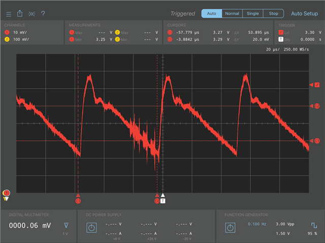
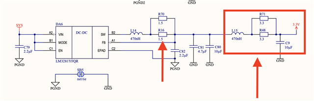
According to the datasheet, the ripple of ~60mV is the normal way how LM3281YFQR operates in the ECO mode. But the problem is that we cannot have this level of ripple because our MCU requires more clean power for it's BLE connectivity. So we try to make the voltage ripple of DCDC more smooth by adding those resistors and additional inductor (see read arrow below) before MCU VDD input:.
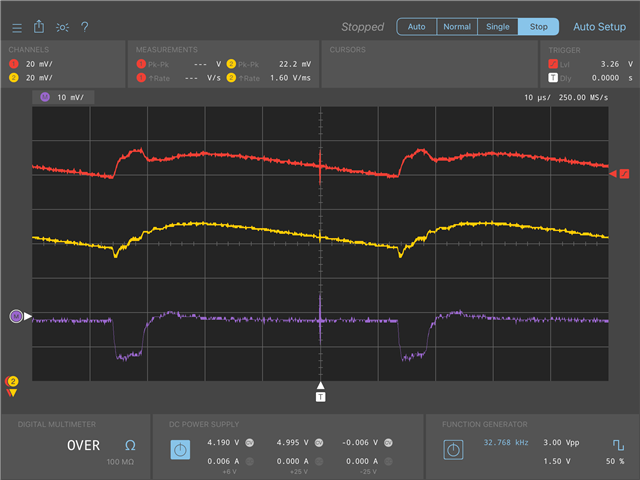
After this the output ripple becomes smaller (yellow line) and our MCU can work normally.
Our question is if it's okay for LM3281YFQR to have those additional components after it's output because this schematic design is different from the one recommended by the datasheet. Can u help to confirm it?
Thanks,
Best Regards
