- Ask a related questionWhat is a related question?A related question is a question created from another question. When the related question is created, it will be automatically linked to the original question.
Hello,
We are trying to amplify a sine wave pwm (generated by a TMS570) using the LMG1205HBEVM evaluation board.
We noticed an abnormally high current with the default EVM board when testing this.
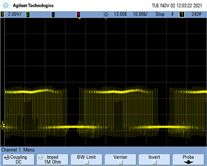
To try and determine the cause we first did a reference test connecting a function generator straight to the EVM board:
So power consumption is as expected here in this first test.
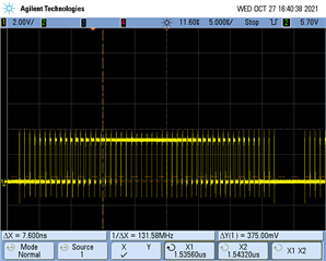
Then we did a test with the sine wave pwm generated by the TMS570:
Below are some screenshots of this second test:
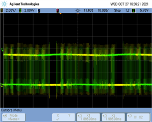
Yellow signal = measured on LO (TP11)
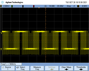
Fig 1: PWM freq = 1 Mhz for building a sine wave
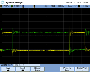
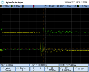
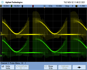
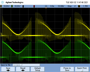
Yellow signal = measured on LO (TP11)
Green signal = measured on HO (TP3)
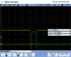
Fig 2: dead-time between LO-HO (with modulated PWM)
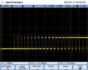
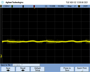
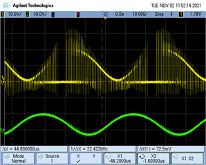
Yellow signal = measured on LO (TP11)
Green signal = measured on HS (TP12)
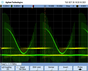
Fig 3: result on output
Questions:
Any help is appreciated.
Kind regards,
Geert Jacobs