This thread has been locked.
If you have a related question, please click the "Ask a related question" button in the top right corner. The newly created question will be automatically linked to this question.
Hi engineers,
I have some questions about Cdv/dt calculation:
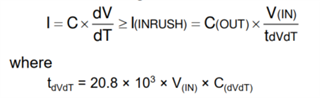
Formula show as blow:
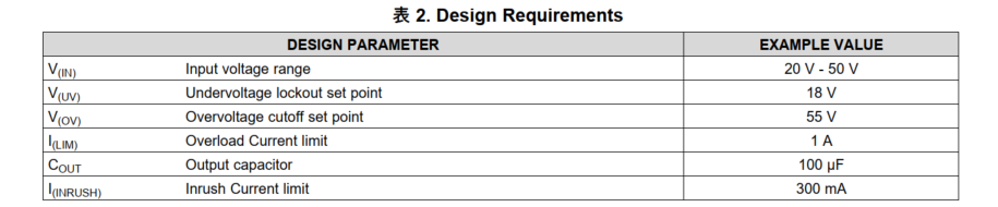
A application case design requirement in datasheet show as blow:
calculation result is Cdv/dt =22nF,
question1:What is the detailed and complete calculation process to figure out 22nF?
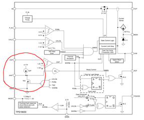
The IC structure diagram show as blow
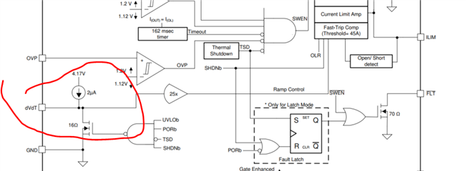
question2:How the Cdv/dt maintain fixed dv/dt(slew rate) during power up process?(such as :what's the function of 2uA CCS and 25 gain section)
question3:As my observes, the Cdv/dt is similar with Ct in load switch, So do the two things have the same function?
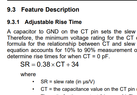
question4:How to deduce SR formula of TPS22965?
Correct picture, the application case design requirement in datasheet show as blow:
Hi Stanley,
A1) During startup, the device controls the GATE voltage in proportional to the voltage on the dVdT pin
It uses simple I=C*dv/dt relation
Iinrush = Cout *Vout/tdVdT (at the end of power-up Vout = VIN) => Iinrush = Cout *VIN/tdVdT -- (1)
tdVdT = 20.8 × 10^3 × VIN × CdVdT ---(2)
Equation (2) in the data sheet is arrived by design and by doing the curve fitting the results.
Now with 100uF (Cout) and to limit Iinrush to 300mA
Using (1) & (2), we get CdVdT = 16 nF => selected 22nF nearest higher value
A2) During startup, the GATE is controlled as source follower to maintain constant slew-rate of the voltage
A3) Yes, ct in load switch and CdVdT in eFuses are similar in function
A4) These equations are arrived by design and by doing the curve fitting the actual results.
Hi Rakesh, I'm TI fae NCG, can I get your email address to discuss understanding about the feature of dv/dt start-up which I'm very curious about.
Hi Stanley,
We are not fully aware of internal design details. Sure, you can reach me on email to discuss further.
Best Regards, Rakesh