This thread has been locked.

If you have a related question, please click the "Ask a related question" button in the top right corner. The newly created question will be automatically linked to this question.

UCC28740: DC-DC Flyback converter for wide input range

Part Number: UCC28740
Other Parts Discussed in Thread: TL431, , LM5021

Hi there,

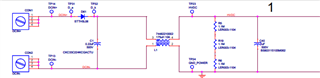
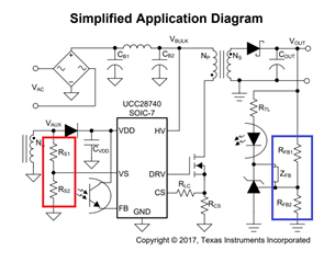
I am willing to design similar product for diffirent input range, https://www.ti.com/tool/UCC28740EVM-525

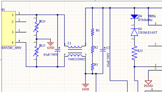
INPUT: 250 to 650 VDC
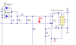
OUTPUT: 24V/5A

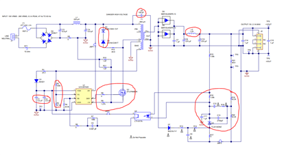
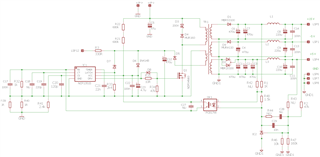
Kindly suggest me to change the schematics ( reffrence design from above link)  below,

1. I want to remove the input bridge diode part, could you tell me does D4 and D3 has include for AC input in primatry side of transformer ?

2. My input may vary from 250 to 650 VDC, so R2, R3 value should keep according to equation 1 and 2 of datasheet UCC28740? Does it mean input range should be fixed ?

3. My MOSFET should be 900VDC, how about change it to  TU7NM90N?

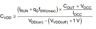
4. Explain to change C6 value.

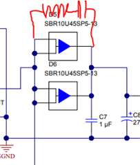
5. Suggest to calculate output inductor and capacitors , C7,C8, L2,C10, C14,C15.

6. Describe to calculate protection circutity C12,R8, C13.

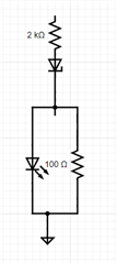
7. By the voltage divider rules, R2-R21 has been calculate right?

8. to sencing the R16 value, LTV -817 is okay for 24V/5A application?

  • Hi, 

    Thanks for reaching us. 

    Please check my reply as below. 

    1. When input is DC, you may remove D2 which is a bridge rectifier. It is still needed to keep D3 and D4 since they are used to absorb VDS spike during MOSFET switching. You may modify their value based on input voltage range and transformer design. 

    2.  R2 and R3 would be calculated by equation1 and equation 2 but they are not fixed value. It is needed to re-design according to VIN(RUN) and Vovp that your system specified.  

    3.  I could not find the datasheet of TU7NM90N. Please note the VDS rating must be higher than Vin(max) + nVoutout at least.  where n is Np/Ns. Normally it is needed to have 20%~30% margin. i.e. The Vin,max is 650V, Voutput is 24V. Assumed n is 8, the VDS rating is 650V+8*24 = 842V (at least). Consider 20% margin, it is needed to choose VDS=1.2*842V=1010.4V --> You may need to choose 1200V MOSFET. 

    You may refer the calculation tool as below link to design the component values. 

    UCC28740 Design Calculator.

    4. C6 is Y-cap which is used to improve EMI.  The value is not fixed. You may modify it based on the EMI test results. 

    5. Please refer the calculator as above. L2 is an option, which is a way to improve output voltage and current ripple.

    6. C12, R8 and C13 are designed to feedback compensation. To adjust them to optimize the gain/phase margin. You may design them through the calculator.

    7. Sorry I may not sure I understand well about your question. Are you asking how to calculate R2-R21? If yes, you could calculate R2-R21 according to the equations on UCC28740's datasheet, or get them through the calculator. 

    8. LTV-817 is not used to sense R16's voltage. It is used to send feedback information to primary side. R16 is used to provide an additional current to supply TL431.

    Please let me know if you have other questions. 

    Thanks. 

    Regards, 

    Wesley

  • Dear Sir Wesley,

    Thank you very much for your response. It is indeed resonable and valuable for design.

    Now looking at your response, lets put my feedback one by one.

    1. When input is DC, you may remove D2 which is a bridge rectifier. It is still needed to keep D3 and D4 since they are used to absorb VDS spike during MOSFET switching. You may modify their value based on input voltage range and transformer design. 

    1. Yes, I removed the rectifier part and put a sutable circuirity as follows. Now question is how to select L and R values. 

    For, D3 I have chosen , https://static6.arrow.com/aropdfconversion/a67d6e48675e652f4953d4194c42b2fe52a54c55/littelfuse_tvs_diode_tpsmb_datasheet.pdf.pdf

    and D4 should be same https://www.mouser.com/datasheet/2/427/VISH_S_A0010476682_1-2571149.pdf

    2.  R2 and R3 would be calculated by equation1 and equation 2 but they are not fixed value. It is needed to re-design according to VIN(RUN) and Vovp that your system specified.  

    2. Well said, I have calculate R2 as 71k and  R3 =209.6 k arrording to equation 1 and 2, I consider Vovp = 24V , Vin(run)=650VDC

    3.  I could not find the datasheet of TU7NM90N. Please note the VDS rating must be higher than Vin(max) + nVoutout at least.  where n is Np/Ns. Normally it is needed to have 20%~30% margin. i.e. The Vin,max is 650V, Voutput is 24V. Assumed n is 8, the VDS rating is 650V+8*24 = 842V (at least). Consider 20% margin, it is needed to choose VDS=1.2*842V=1010.4V --> You may need to choose 1200V MOSFET. 

    You may refer the calculation tool as below link to design the component values. 

    UCC28740 Design Calculator.

    Well noticed, but unfortunately your calculator does not working as exel file, codes are not active. I managed to calculate Nps(max) from equation 13, in my case its 33 but I am not sure how to calculate Ns and Np individually. Normal flyback case its defined as Ns= Vin_max(SQ) * D_max/ (1-Dmax)* (Vout+Vd). Kindly refer me any particular equation.

    How about this MOSFET, https://www.mouser.com/datasheet/2/196/Infineon_AIMW120R035M1H_DataSheet_v01_00_EN-2329026.pdf

    4. C6 is Y-cap which is used to improve EMI.  The value is not fixed. You may modify it based on the EMI test results. 

    Can you recommend anything within my range?

    . Please refer the calculator as above. L2 is an option, which is a way to improve output voltage and current ripple.

    Let me calculate current ripple then.

    Can you recommend any quation considering the input capacitor voltage? From equation 11, I used to manage Cbulk, for Vin=250 , Cbulk= 0.0021F and for Vin=650, Cbulk= 6.64uF.

  • Hi, Mr. Hasan:

    Please check my reply as below. 

    1. May I know why you put a common choke (L) ? would you please share me your concept? 

    For D3 and D4, please check the voltage rating once you finish the transformer design

     2. Vovp should be higher than Vo. Since the Vo is 24V, I would like to suggest you to use 28V~30V for Vovp. 

    *if Vovp = Vo, the IC would enter to the protection mode when output raise to the target voltage. 

    3. It is strange that I tested the link. The excel should be workable.  Or you may find the calculation tool in https://www.ti.com/product/UCC28740#design-tools-simulation. Please download the calculator. It would save some time for the design process. 

    1200V SiC MOSFET is okay but please consult the supplier because some SiC MOSFET needs to be turned by negative DRV voltage. It is helpful to get the supplier's suggestion to make it operate well.  Another way is to use casecode topology as below. You could use 2 600V or 650V MOSFETs to meet the 1200V rating. 

    https://e2e.ti.com/blogs_/b/powerhouse/posts/design-considerations-of-high-voltage-converters-in-a-cascode-mosfet

    4. For Y-cap vaule, you may start from 100pF~220pF. 

    5. Please use the minimum input voltage to design bulk capacitor. In this case, DC=250V is the minimum input, so please use DC=250V to make sure the capacitance is enough. 

    Regards, 

    Wesley

  • Dear Sir Wesley,

    I am busy on other work. I will come up with feedback soon.

  • Dear Sir Wesley,

    Sorry fro my late response.

    Here we go....

    1. May I know why you put a common choke (L) ? would you please share me your concept? 

    Common mode choke coils are suited for noise suppression on lines with large current flows, . The distortion of the waveform is less. Common mode choke coils are suited for noise suppression on lines where signal waveform distortion causes a problem,

    For D3, previoud linked diode not matched ? It has 700 VDC+ and high current capacity. D4 is also suitable.

    2. Vovp should be higher than Vo. Since the Vo is 24V, I would like to suggest you to use 28V~30V for Vovp. 

    *if Vovp = Vo, the IC would enter to the protection mode when output raise to the target voltage. 

    Yes, I have calculated R2= 71.62 k and R3= 98.74k (Npa=33, Ivsl=275uA, Nas=0.35, Vovp=30V)

    1200V SiC MOSFET is okay but please consult the supplier because some SiC MOSFET needs to be turned by negative DRV voltage. It is helpful to get the supplier's suggestion to make it operate well.  Another way is to use casecode topology as below. You could use 2 600V or 650V MOSFETs to meet the 1200V rating

    Lets use 1200V one, I will see its negative DRV voltage.

    5. Please use the minimum input voltage to design bulk capacitor. In this case, DC=250V is the minimum input, so please use DC=250V to make sure the capacitance is enough.

    Rellay its comming some strange value, Cbuck(min)= 0.0021 F( Pin=131.86, Vin(min)=250v, Vbuck(min)=250v, f-line=47Hz)

    Cbuck(max)= 6.64uF  (Pin=131.86, Vin(max)=650v, Vbuck(max)=650v, f-line=47Hz)

    I also calculate 1. Output diode voltage, Vdk= 61.1V, 

                             2. on time Dmax= 0.52 ( Dmagcc=0.425,tR= 10 ^(-6),f-max= 100kHz,

                             3. Nps (max)= 33

                             4, current-sense resistor, Rcs= 1.07R,( Vccr=243mV, Iocc=343mA, nXMFR=0.91  )

                             5. series resistor Rcl=1.13k

                             6. transformer primary peak current. Ipp(maz)= 0.75 A, 

                             7. primary transformer inductance, Lp= 4.6mH.

                           Give me some idea to calculate Cout.

  • Hi, Mr. Hasan:

    Thanks for your reply. 

    I would like to share some of my opinions about your design. 

    1. Choose fs. 

    As your design, fs is 100kHz, which is the max frequency of UCC28740. I would like to suggest you to use smaller value, i.e. 80kHz. 100kHz is the maximun fs of UCC28740. So if it is set fs=100kHz as full load. IC would enter to CC mode once the output loading is higher than full load. Normally it is suggested to have some margin to any load condition unexpected. 


    2. Nps:

    As you mentioned you are using Nps is 33, it seems too big to use. As it is a flyback topology, there would be a reflect voltage from Vo when MOSFET turns off. The reflect voltage could be calculated as Nps*Vo. Hence, if the Nps is 33. The reflect voltage would be 33*24V=792V. To consider the max input voltage is 650V. The total voltage would be 650V+792V=1442V on your MOSFET when the MOSFET turns off. It is over 1200V rating of SiC MOSFET. You may need to reduce the Nps to meet the SiC MOSFET's voltage rating. 

    As 1200V MOSFET is chosen, the Nps should be less than 22.  Please consider to use18~20 for this design. 

    Some parameters might need to be modified when Nps is changed.

    3. For Cout calculation, it depends on the what ΔVo that you need during the Iout,step. The equation would be 

    Cout ≥ Io,step*tresp/ΔVo  

    For example, assume Io,step is 1A,  tresp = 1ms, ΔVo=1V, The Cout = 1A*1ms/1V = 1000uF

    Regards,

    Wesley

  • Dear Sir Wesley,

    Very empassive feedback indeed. You went insight very technically. I have to go throuh this datasheet again.

    1. Choose fs. 

    As your design, fs is 100kHz, which is the max frequency of UCC28740. I would like to suggest you to use smaller value, i.e. 80kHz. 100kHz is the maximun fs of UCC28740. So if it is set fs=100kHz as full load. IC would enter to CC mode once the output loading is higher than full load. Normally it is suggested to have some margin to any load condition unexpected. 

    Yes, well said. I should not take bellow 100kHz. CC mode is very imporatant, lets say fs=80kHz.

    2. Nps:

    As you mentioned you are using Nps is 33, it seems too big to use. As it is a flyback topology, there would be a reflect voltage from Vo when MOSFET turns off. The reflect voltage could be calculated as Nps*Vo. Hence, if the Nps is 33. The reflect voltage would be 33*24V=792V. To consider the max input voltage is 650V. The total voltage would be 650V+792V=1442V on your MOSFET when the MOSFET turns off. It is over 1200V rating of SiC MOSFET. You may need to reduce the Nps to meet the SiC MOSFET's voltage rating. 

    As 1200V MOSFET is chosen, the Nps should be less than 22.  Please consider to use18~20 for this design. 

    Some parameters might need to be modified when Nps is changed.

    Nice explanation and it is reasonable. One expart says, "You want 160 to 200 watts.
    I think you can use almost any 110-220 ac circuit for a start. Increase the voltage on the MOSFETs. Decrease the current some. Change the turn ratio on the transformer. (increase the primary turns) Increase the inductance. It should work.

    220vac makes 308vdc Your dc voltage is 650 max. So I think you need 2X the voltage and 1/2 the current on the primary side. Those numbers are crude but will get you close. For a simple flyback you might be up against 1000V MOSFETs. Another option is half bridge where 750 to 800V MOSFETs will be save."

    Looking at the datasheet 13 equation, Nps(max)= 13 ( close to), Dmax=0.53, Vbuck(min)=250V,  Dmagcc=0.425, (Vocv+Vf+Vocbc)=24V.

    Lets take Nps=20 then. Refelect voltage is a big issue, since MOSFET is facing more than 1200V.

    3. For Cout calculation, it depends on the what ΔVo that you need during the Iout,step. The equation would be 

    Cout ≥ Io,step*tresp/ΔVo  

    For example, assume Io,step is 1A,  tresp = 1ms, ΔVo=1V, The Cout = 1A*1ms/1V = 1000uF


    Great ! Few things are confusing, do you assume this  step as transient response? In my case what values are suitable? 

    Now again the modified calculations are as follows, Cout= 6.64uF,  R2= 118.18 k and R3= 1.5M (Npa=20, Ivsl=275uA, Nas=0.35, Vovp=30V)

                              1. Output diode voltage, Vdk= 80v, 

                             2. on time Dmax= 0.53 ( Dmagcc=0.425,tR= 10 ^(-6),f-max= 80kHz,

                             3. Nps (max)= 20 

                             4, current-sense resistor, Rcs= .65 R,( Vccr=243mV, Iocc=343mA, nXMFR=0.91, Nps=20  )

                             5. series resistor Rcl=1.5k

                             6. transformer primary peak current. Ipp(maz)= 1.24 A, 

                             7. primary transformer inductance, Lp= 2.1mH.

                             8. minimum on time of the MOSFET (ton)= .78us ( sqr2 is included)

                             9. minimum demagnetization time  of the transformer, tdm= 1.4us


  • Hi, Mr. Hasan:

    Great ! Few things are confusing, do you assume this  step as transient response? In my case what values are suitable? 

    Yes, it is transient response. The spec. depends on your system specification.  0.5A ~ 1A could be a start if you have no specific request of transient responses. 

    Regards, 

    Wesley 

  • Dear Sir,

    Thank you.

    Lets say its 1000uF. Any voltage equation you know relating capacitor voltage of  Cbuck(max) or Cout? I used Vbulk(max)=650 v, so 700v is okay?

    Since output is 24V then how about 1000uF/50V? 

    I have few more query .

    Here we go,

    1. Your eval board, UCC28740EVM-525 10 W does not contain any resistor that might required from gate to drain of  MOSFET Q1. Kindly explainit more.

    2. Does your supplied document contains feedback compensation calculation ? Kindly guide me how I can set them for my requirment.

    3. Shunt sensing part also need to calculate.

    4. At filtering part L2 and C7 need to calculate.

    5. At EVM board, R13, R14 and C9, D7 has not solder, kindly explain.

    6. For my power range, 1200V MOSFET does not need heatsink?

  • Dear Mr. Hasan:

    Lets say its 1000uF. Any voltage equation you know relating capacitor voltage of  Cbuck(max) or Cout? I used Vbulk(max)=650 v, so 700v is okay?

    Since output is 24V then how about 1000uF/50V? 

    There is no equation as I know. We only need to check the voltage rating is higher than it needs. So it is okay to choose 700V for 650V input and 50V for 24Vout. 

    1. Your eval board, UCC28740EVM-525 10 W does not contain any resistor that might required from gate to drain of  MOSFET Q1. Kindly explainit more.

    I think you are asking the resistor between gate-source? ( use a resistor to connect gate-drain would make MOSFET always ON.)

    Since it is an evaluation board, and the power is only 10W. It has less risk for MOSFET gate signal distortion. However, in real projects, I will recommend you to put it to improve gate operation. 

    2. Does your supplied document contains feedback compensation calculation ? Kindly guide me how I can set them for my requirment.

    Please check the feedback compensation of UCC28740 as below. 

    Practical Feedback Loop Design Considerations for Flyback Converter Using UCC28740

    3. Shunt sensing part also need to calculate.

    You can use the CS resistor calculation as below. It also has detail description on page 11 in UCC28740's datasheet. 

    4. At filtering part L2 and C7 need to calculate.

    L2 and C7 are formed as a LC filter. Once Cout is calculated, you could use this value to get the L2 based on the LC filter design. 

    5. At EVM board, R13, R14 and C9, D7 has not solder, kindly explain.

    It is just a kind of external softstart circuit. It is an option but not necessary. 

    6. For my power range, 1200V MOSFET does not need heatsink?

    I would like to suggest you to keep the heatsink in the initial stage. since it is hard to estimate the switching loss and conduction loss which are impact by stray inductance and capacitance. 

    May I know what's your end application? Is this power for a battery charger?

    Thanks. 

    Regards, 

    Wesley

  • I think you are asking the resistor between gate-source? ( use a resistor to connect gate-drain would make MOSFET always ON.)

    Since it is an evaluation board, and the power is only 10W. It has less risk for MOSFET gate signal distortion. However, in real projects, I will recommend you to put it to improve gate operation. 

    Do you mean I need to  add a resistor to  gate-source? How about 10k ?

    You can use the CS resistor calculation as below. It also has detail description on page 11 in UCC28740's datasheet. 

    I have calculated Rcs = 0.65 R, ( Vccr=343mV, Iocc=5A, nXFMR=0.91, Nps=20)

    Rlc=1.5k( Klc=28.6, Rs1=118.18k, td=72ns, Lp=2.1 mH)

    I would like to suggest you to keep the heatsink in the initial stage. since it is hard to estimate the switching loss and conduction loss which are impact by stray inductance and capacitance. 

    May I know what's your end application? Is this power for a battery charger?

    Yes, lets add a heatsink, Yes this is for PV battery charger

  • Hi, Mr. Hasan

    Do you mean I need to  add a resistor to  gate-source? How about 10k ?

    Yes. 10k~33k would be okay. 

  • Thank you sir Wesley.

    Can you recommend a flyback transformer similar to your design but within my range? Which equation you used to calculate secondary transfor winding Ns?

  • Hi, Mr. Hasan:

    I think I could not design a transformer according to our EVB's size since the power rating is much different from yours (10W vs. 120W)

    you may consult your transformer vendor to pick up the suitable size and suitable core. Then you can use the equation Nsec = Lp*Ipeak/(Nps * Bm* Ae) to get the Ns. Then you could use Ns to get Np and Naux. 

    I still recommend to check your design through the attached calculator. It can work normal in my laptop . This calculator is easy to use to verify these value are proper or not. 


    8561.sluc487b.xlsx

    Regards, 

    Wesley.

  • I think I could not design a transformer according to our EVB's size since the power rating is much different from yours (10W vs. 120W)

    you may consult your transformer vendor to pick up the suitable size and suitable core. Then you can use the equation Nsec = Lp*Ipeak/(Nps * Bm* Ae) to get the Ns. Then you could use Ns to get Np and Naux. 

    I still recommend to check your design through the attached calculator. It can work normal in my laptop . This calculator is easy to use to verify these value are proper or not. 


    Really you have helped me a lot!

    Thank you once again. Now calculation is accurate, I am doing PCB work for this design, it has high current in output so traces need to be wide enough.

  • Hi, Mr.Hasan:

    Glad to hear that. Please click the answered if your questions are solved. And you can open another thread when you meet other issues.

    Regards,

    Wesley

  • Dear Sir Wesley,

    I have few more query, 

    1. My boss want me to put some common ground ZNR” Transient/Surge Absorbers, in folloing manner, https://www.farnell.com/datasheets/2244565.pdf

    2. I dont think he need it for protection since there is 2 cap, 1 noise suppreser and rersistor is available.

    3. He wants to add a fuse in pin 1 to R24, not sure really.

    4 Can you imagine any idea to use R1-3? Those are 1 Mohms.

    5. He talks about the snubber in secondary output, where D5,D6 are connected. 

    6. He wants to add a LED indecator for power, for 5A current I dont think any simple way. Kindly give a TI solution.

  • Hi, Mr. Hasan:

    For ZNR, the protection speed is faster than capacitor and can absorb higher surge energy than capacitor. So if your input source is not stable or it has some special condition would cause a surge input to the converter. A ZNR is a good solution to protect your circuit. One thing make me curious is you mentioned this is a solar charger, and the input is 250Vdc ~ 850Vdc. So my guessing is the converter uses a battery as an input. I am not sure if the battery has this kind of condition.  Maybe I was wrong. Would you please share it to me?  

    Since I do not understand the real condition very well. You may also check if your converter has the plan to apply the safety standard. If yes, you need to add the ZNR in input side.  

    3. He wants to add a fuse in pin 1 to R24, not sure really.

    I can not find the R24 in our EVB's schematic, and Pin1 is Vcc. I could not commend this. Please share me the schematic or point out where R24 is. Thanks. 

    4 Can you imagine any idea to use R1-3? Those are 1 Mohms.

    These resistors are used to discharge C2 faster. I think it prevent someone not to get an electric shock when he touches the board or input side when C2 is not totally discharged.  

    5. He talks about the snubber in secondary output, where D5,D6 are connected. 

    You can add RC in parallel as below to be a snubber. 110ohm with 100p might be a good start. To optimize them based on the real test results. 

    6. He wants to add a LED indecator for power, for 5A current I dont think any simple way. Kindly give a TI solution.

    If it only needs if the converter power on or not, just add a LED and a resistor in series at output side as below. 

    Regards,

    Wesley

  • Dear Mr. Wesley,

    Thank you once again.

    Take a look this figure,

    Let assume pin 2 and 3 are not connected, R24-25 is just symbolic. You can assume a resistor like symbol.

    1. R24 and R25 are transient voltage protectors, so additional transient protectors are not needed?

    These resistors are used to discharge C2 faster. I think it prevent someone not to get an electric shock when he touches the board or input side when C2 is not totally discharged.  

    Discharging resistor values are ok? Do you want me to see here, http://hyperphysics.phy-astr.gsu.edu/hbase/electric/capdis.html. Yes, Without them a person could have a very dangerous shock if they touched the two convertor's power plug pins after being unplugged..

    You can add RC in parallel as below to be a snubber. 110ohm with 100p might be a good start. To optimize them based on the real test results.

    Snubber circuit need to calculate well. I dont think those diode will get large dv/dt transient, since built in diode has enough barrier. what do you think?

    If it only needs if the converter power on or not, just add a LED and a resistor in series at output side as below. 

    Great idea, with a LED indicator on the output leads so one can see that the converter is likely putting out charging power. A 5K resistor in series with a LED would show if any voltage is present at the output (before it is connected to a battery). A 24-V 1W zener in series with a 2K resistor to the LED (with a 100-ohm in parallel with the LED) would show that the voltage is near the proper level, but either way the LED would not show if any current is flowing out to the batteries to be charged.

  • Hi, Mr. Hasan:

    Let assume pin 2 and 3 are not connected, R24-25 is just symbolic. You can assume a resistor like symbol.

    Are they varistors? Varistors' function is similar to ZNR but ZNR is faster than varistors 

    Sorry I am not so familiar about your application but you may use each of them (or both) for different safety standard requirement. 

    Discharging resistor values are ok? Do you want me to see here, http://hyperphysics.phy-astr.gsu.edu/hbase/electric/capdis.html. Yes, Without them a person could have a very dangerous shock if they touched the two convertor's power plug pins after being unplugged..

    Usually it is needed to discharge capacitor's voltage to below 60V in a second. So you may design discharging resistance based on the principle if there is no definition in your system yet. 

    Snubber circuit need to calculate well. I dont think those diode will get large dv/dt transient, since built in diode has enough barrier. what do you think?

    There could be a high di/dt as output short condition. So I thought you could keep the snubber's space when you are doing PCB placement, just in case, the higher voltage stress caused by the di/dt when it happens.

    Great idea, with a LED indicator on the output leads so one can see that the converter is likely putting out charging power. A 5K resistor in series with a LED would show if any voltage is present at the output (before it is connected to a battery). A 24-V 1W zener in series with a 2K resistor to the LED (with a 100-ohm in parallel with the LED) would show that the voltage is near the proper level, but either way the LED would not show if any current is flowing out to the batteries to be charged.

    I think the LED still can work when it connects to batteries because this LED is used in parallel to batteries. So current still flows to LED even battery is fully charged. 

    Regards, 

    Wesley

  • Dear Sir Wesley,

    Thank you again.

    I want to know few rgent questions.

    1. As my input ranges 250-650VDC, then if I set all control resistor for 650V then dous it work for 250VDC also? 

    2. How do you calculate R1? I used equation 1, where Ivsl=275uA,Npa=33, it comes like 71k in my case.

    3. I had few confusion to calculate Np and Ns, from your iven formula  Nsec = Lp*Ipeak/(Nps * Bm* Ae), Np= 494 and Ns=15( kindly check your formula, its for Ns?)

    4. Suggest me how to calculate, R19-R21.

    Sorry if these question went wrong.

  • Hi Mr. Hasan:

    Please check my reply as below. 

    1.  It depends on which resistors you are asking. For Rs1 and Rs2 as below, it is needed to use 250Vdc input. 

    2. What's the Vin(run) you chosen?

    Assumed Vin(run) is 250Vdc, IVSL=275uA, and Npa is 33. consider the equation on page 10 in datasheet. 

    Rs1 = 250Vdc/(33*275uA) = 27.54kohm. 

    The 71kohm comes from 650VDC. It means IC would start once VDCinput is 650V. So it can not be used. 

    3.  The formula would be

    set Nps=Np/Ns => Ns = Np* 1/Nps 

    Lp * Ipeak = Np * Bsat * Ae  => Np = Lp * Ipeak / (Bsat * Ae) 

    So  Ns = Lp * Ipeak / (Nps*Bsat*Ae) . the formula is correct I think. 

    You may find more detail about transformer design as the link: Inductor and flyback transformer design.

    *According to your calculation, the Ns=15 and Np= 494, so the Nps = 494/15 = 33. As we talked, if you choose Nps=33, the reflect voltage would be 24*33=790Vt, and your max input voltage is 650V. The max voltage on Vds (not include voltage spike) is 1440V. It is over your 1200V SiC MOSFET rating if you still keep using the same specification SiC MOSFET you chose. 

    * The Np should be 300 turns if you chose Nps = 20. 

    4,  Is the R19-R21 are equal to RFB1 and RFB2?

    If yes,  it depends what shunt regulator that you choose. 

    Assume Vref = 2.495V,  (TL431

    Vo * (RFB2/(RFB1+RFB2)) = Vref. 

    RFB1 = RFB2* ( Vo/Vref -1 ) => you can set RFB2 as 42k just like EVB's, then you can get your RFB1. 

    Regards, 

    Wesley 

  • 2. What's the Vin(run) you chosen?

    Assumed Vin(run) is 250Vdc, IVSL=275uA, and Npa is 33. consider the equation on page 10 in datasheet. 

    Rs1 = 250Vdc/(33*275uA) = 27.54kohm. 

    The 71kohm comes from 650VDC. It means IC would start once VDCinput is 650V. So it can not be used. 

    .

    I was talking about the reference design I posted at first post, R1 values in this figure.

    In my case, Rs1 = 650Vdc/(33*275uA)= 71.62k, it is similar to R1? Since R2 is parallel with it and primary winding current is assciated.

    Does it means for 250VDC R1= 27.5K and for 650VDC, R1= 71.6k.

    Here  is the main disadvantage of this design that, wide range is not applicable. For different input different values should be consider.

    As we talked, if you choose Nps=33, the reflect voltage would be 24*33=790Vt, and your max input voltage is 650V. The max voltage on Vds (not include voltage spike) is 1440V. It is over your 1200V SiC MOSFET rating if you still keep using the same specification SiC MOSFET you chose.


    That means R1 aslo changes for Np=300,Nps= 20, Ns= 15

    4,  Is the R19-R21 are equal to RFB1 and RFB2?

    If yes,  it depends what shunt regulator that you choose. 

    Assume Vref = 2.495V,  (TL431

    Vo * (RFB2/(RFB1+RFB2)) = Vref. 

    RFB1 = RFB2* ( Vo/Vref -1 ) => you can set RFB2 as 42k just like EVB's, then you can get your RFB1. 

    Regards, 

    I do mean R19, R20 and R21, Upper figure shows RFB1..2 = R15, R16 may be.

    For R19, R20 and R21 voltage divider rull is not applicable? Calculate them please. if I chose Vin=24V, I=5A, R21+R19=2 R20, then,  R21+R19= 3.2 R, R20=1.6 R, may be I am doing wrong.

    If I use a heatsink then its bottom pin should be connect with GND? It means its drain should be in GND.

  • Hi, Mr. Hasan

    In my case, Rs1 = 650Vdc/(33*275uA)= 71.62k, it is similar to R1? Since R2 is parallel with it and primary winding current is assciated.

    Does it means for 250VDC R1= 27.5K and for 650VDC, R1= 71.6k.

    Here  is the main disadvantage of this design that, wide range is not applicable. For different input different values should be consider.

    The formula of RS1 is fixed and shown in datasheet.  Npa of EVB is different from yours, thus, the RS1 value is different. 

     Vin(run) means the min input voltage to turn on the converter. Thus, it is not able to use 650VDC to do this calculation. It should be 250Vdc as your spec. 

    That means R1 aslo changes for Np=300,Nps= 20, Ns= 15

    Yes. 

    Assume Vref = 2.495V,  (TL431

    Vo * (RFB2/(RFB1+RFB2)) = Vref. 

    RFB1 = RFB2* ( Vo/Vref -1 ) => you can set RFB2 as 42k just like EVB's, then you can get your RFB1. 

    This equation still follows KVL.  R21 is used to optimize the output voltage, any way, The output voltage setting follows the equation as above.  

    In EVB, as output is 5V.  TL431A whose Vref=2495V is chosen. 

    Choose R20 = 42.2kohm. 

    (R19+R21) = 42.2kohm ( 5/2.495 - 1) = 42.369kohm. 

    So in your case, assume TL431A is also chosen. Vout is 24V.  Keep R20 is 42.2kohm. 

    (R19+R21) = 42.2kohm (24/2.495-1) = 362kohm. 

    If I use a heatsink then its bottom pin should be connect with GND? It means its drain should be in GND.

    It is needed to put an insulator between your MOSFET and heatsink if the package is not insulated.

    Regards, 

    Wesley

  • The formula of RS1 is fixed and shown in datasheet.  Npa of EVB is different from yours, thus, the RS1 value is different. 

     Vin(run) means the min input voltage to turn on the converter. Thus, it is not able to use 650VDC to do this calculation. It should be 250Vdc as your spec.

    Do you mean even if 250 V is used to calculate, the system will allow 650V input also? You said nothing about R1. According to figure, my R2=45.45k, R3=62.66k.

    It is needed to put an insulator between your MOSFET and heatsink if the package is not insulated.

    I do mean the bottom pin of heatsink. My PCB has no GND trace near heatsink. I did see one design where heatsink is grounded with panel ground. Yes I will use insulating pest over the heatsing and MOSFET pad.

  • Do you mean even if 250 V is used to calculate, the system will allow 650V input also? You said nothing about R1. According to figure, my R2=45.45k, R3=62.66k.

    Yes. it is also available as 650V input.

    Heatsink connects to GND can reduce EMI normally, so it is suggested to connect heatsink to GND. 

    Regards, 

    Wesley

  • Heatsink connects to GND can reduce EMI normally, so it is suggested to connect heatsink to GND.

    Yes, I know it. Even if I dont connect then what would be the problem? I forget to ask you C1 and C2 values. 

    Secondly, can you suggest any IC that is applicable for muilti output like 5V/3A, 12V/2A with 250-650VDC input? DC-DC converter.  

  • If the heatsink does not connect to GND, it would be full of switching noise since it is closed MOSFET's drain. So it might impact the component around it. 

    For C1 and C2, both they are VDD's capacitors. So you can get C1+C2 through the equation as below. 

    And the detail description is on page 23 in datasheet. 

    Are you looking for non-isolated or isolated solution?

    You can check the reference design first as the link. 

    TI Reference Designs Library

  • For C1 and C2, both they are VDD's capacitors. So you can get C1+C2 through the equation as below.

    Happy new year 2022. You helped me a lot. Yes, I got 32.2uF in total . Lets assume 16uF for each.

    And the detail description is on page 23 in datasheet. 

    I am really sorry. I should loot at it at least.

    Are you looking for non-isolated or isolated solution?

    I think its should be isolated. Lets me show you a similar design. May be transformer need to be modify.

  • Hi, Mr. Hasan:

    Please refer the PMP30495. with LM5021 which is a CCM flyback controller, and the transformer need to redesign because of the different power rating. 

    Regards, 

    Wesley

  • Hi, Mr. Hasan:

    The most different between each of them are controller and transformers. 

    I am sorry I have no controller price information here, and neither does transformers. 

    So maybe you can contact your TI sales window to get the controller price. 

    Sorry and Thanks. 

    Regards, 

    Wesley

  • The most different between each of them are controller and transformers. 

    I am sorry I have no controller price information here, and neither does transformers. 

    So maybe you can contact your TI sales window to get the controller price. 

    I see. May be topology is same. Let me study more, TI solution perhaps suitable.

  • All of them are CCM flyback topology. 

    If you need assistance of LM5021 or CCM flyback. Please create another thread. Let's keep the UCC28740 project here. 

    Thanks. 

  • All of them are CCM flyback topology. 

    If you need assistance of LM5021 or CCM flyback. Please create another thread. Let's keep the UCC28740 project here. 

    Thank you sir.

    I will start a new thread for sure but LM5021 works only  8-30V?

  • 8-30V is only for VDD rating. LM5021 is able to be used in much higher input. i.e. PMP30495 Schematic noted the input voltage is 100VDC-623VDC.

  • Well said. My range is little bit hire, but may be manageable. 

  • Yes. 650Vdc input is okay to the design.