This thread has been locked.

If you have a related question, please click the "Ask a related question" button in the top right corner. The newly created question will be automatically linked to this question.

BQ76940: 12s Battery independent cell protection

Part Number: BQ76940
Other Parts Discussed in Thread: TLV810, BQ78350

Hi, 

I had made a previous question about the same topic, as I am looking for a system to be placed between the BMS and each cell of a 12s battery pack balance line. 

Previous question already solved:

https://e2e.ti.com/support/power-management-group/power-management/f/power-management-forum/1046415/tlv810sevm-019-12s-battery-independent-cell-protection

I was trying to make a cell low voltage detection circuit connected to a P channel Mosfet, so the connection between the battery cell is opened in case of undervoltage. The transistor would stop the current draw from the cell in case of BMS board failure. The main component used in the BMS board is BQ76940. 
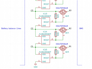
It has been made a prototype of this design, and the system works fine when battery is in rest mode, and also cuts the current flow when there is an undervoltage in a certain cell, but I have problems with this design when balancing. When balancing is being made by the BMS, the current that flows through the balance lines generates a voltage in the Rds of the mosfets, causing a cell reading mismatch by the BQ76940.

The BQ76940 reading sequence is modified when in balance mode, but the current that goes, for example, from the line 5  returns in the line 4, so the reading of the cell 4 gets modified, so the system is not valid as affects the battery voltage monitoring. When the line itself is being balanced,the reading is correct, but the lower line reads 0,2V above the real value, due to the voltage drop produced in the mosfet (about 80mA*Rds).

How is usually made this kind of protection made to protect each battery pack cell, and not interfere with the BMS readings? Could I get any suggestion about how could I modify the circuit to avoid this kind of problems, or would it be better to try a different approach?

Thanks in advance for your time.

  • Hi Adrian,

    I'm not sure where the BMS input filter connects with respect to the schematic clip above. 

    If the circuit is on the BMS side of the filter when the BQ76940 balances the inputs for the cell will pull together causing a low voltage.  This would seem to disconnect the upper input of the IC from the filter which will stop balance current flow.  With 175 ms balance time and 200 ms typical td of the TLV810R the BQ76940 input will likely still be disconnected when the BQ76940 begins balancing, so the voltage will be incorrect. 

    If the circuit above is connected directly to the cell  the supervisor should always see the correct cell voltage and the BQ76940 should remain connected during balancing.  Check that any resistance in the battery interconnect does not provide a voltage which causes the circuit to reset unexpectedly.  Evaluate the circuit to check that the BQ76940 is operated within its recommended operating conditions or at least within its abs max limits.  Also check that the system performance is as desired.  With series connected cells the main current flow in the cells is from one cell to the next rather than from the tap into the BMS board.   In the BQ76940 data sheet  compare IDD with dICELL https://www.ti.com/document-viewer/BQ76940/datasheet/electrical-characteristics-slusbk25983#SLUSBK25983  I expect the circuit would avoid excessive discharge from a situation such as the host setting a cell balance and going to sleep, but would add the IDD load for the supervisor. 

    If you have additional questions on the circuit please include the battery contact and BMS filter component and pin locations in a schematic clip.

  • Hi WM5295,

    First of all thanks for your fast response. 

    The proposed circuit was expected to be placed between the current BMS board and the cells connection. In the following picture can be appreciated the different parts and their placement.

    About the IDD current, as I understand it should be only a problem for the higher cell protection, as it would face a constant voltage shift due to current consumption from the last cell line.

    As you pointed, the problem found in this circuit configuration is the voltage created due to the resistance in the connection between the battery and the BQ76940 VCx input filters, that creates a voltage shift in the reading when the cell above starts balancing. For example, when C2 stars balancing, the voltage reading on the BQ76940 is higher than the real voltage in the cell (about 200mV).

    I did not face problems with the voltage monitor, as it is connector to the cell, but the readings of the BMS are not correct. 

    How could I place a protection device, avoiding that wrong voltage readings due to inline resitance? The mosfet has low on resistance, but a resistance of 2Ohm creates a close to 200mV voltage drop with 100mA of balance current.

    Thanks in advance for suggestion

  • Hi Adrian,

    When balancing a cell in the 3.6 to 4.3V range the voltage of the cell should not change significantly enough from the balance current to change the TLV810 supply/sensing voltage.  So the switch should stay on for all normal cell voltages including balancing operation.  Cells have low source impedance.  You likely can't test the circuit with a resistor divide because it has high impedance and balance current is likely to change the "cell" voltage causing the cell protection board to open its switch.

    The 2 ohm of the protection switch should be negligible in series with the 1k input filter resistor for the BQ76940.  The BQ76940 duty cycles balancing to measure when balance current is not flowing, except at the cell group boundaries. The 2 ohms is also in series with the high current balance path though where it will be in series with the 47 ohm resistor.  At the cell group boundaries you may want to have separate paths for the balance circuits.

    Be sure the BQ76940 has proper voltages during your cell protection board operation.

  • Hi WM5295,

    About your first paragraph of your last response, I agree with that. The TLV810 does not see a significant change in the voltage, as it is connected directly to the cell, that has low impedance. It works properly and is not affected by the balancing process.

    About the BQ76940, as you mentioned, the 2 Ohm of the mosfet creates a voltage divider being in series with the 47 Ohm resistor. That voltage is added to the cell voltage reading, so the voltage reading of the BQ76940 gets modified. The input filter does not modify that reading, as has a higher resistance, but the voltage in front of the filter is already modified.

    As pointed, expected to maybe have problems at cells 5-6 and 10-11, but I also found voltage reading mismatches in other cells, so I dont really understand how could be this avoided, or why is the reading of this cells wrong.

    I tested this problem recording the BMS values using the BQ-Studio and forcing the balance via SMB command (bq78350). 

    Voltage values readed having the protection circuit connected between the BMS and the battery.

    The reading of cells 4,5,8 and 9 get affected by the currents of the balancing process. 

  • Hi Adrian,

    If you have configured the part for 12 cells as shown in the data sheet section 11.1 table 26 https://www.ti.com/document-viewer/BQ76940/datasheet/configuring-alternative-cell-counts-slusbk24812#SLUSBK24812 then the group cell boundaries of the part are between cells 4 and 5 and also 8 and 9.  Common path resistance provided by the switch will form a voltage divider with the other group's cell when balancing as shown in figure 8 of https://www.ti.com/lit/pdf/slua749 In this case the resistance is the FET. 

    To avoid this you need to isolate the currents with separate resistances.  For your situation that could be 2 FETs, but again be sure to keep the inputs for the BQ76940 in safe voltage ranges when the FETs are open.

  • Hi WM5295,

    I had not remembered the cells to bq76940 connections due to the cells number. Now I understand the voltage shift observed from cells 4,5,8,9 during the cells balance process.

    As pointed, I will have to split the VC5, VC5b and VC10, VC10b connections so the balance current only affects the voltage of the group, but does not affect other groups cell voltages. It should be protected the lines VC5 and VC10, and leave the VC5b and VC10b with direct battery connection, as they are only current return path, and that current must not affect other cells.

    Thanks for your support and clarifications.