This thread has been locked.

If you have a related question, please click the "Ask a related question" button in the top right corner. The newly created question will be automatically linked to this question.

TPS40305: Getting the EMI Peaks

Part Number: TPS40305

Hello Team,

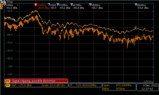
I am getting the EMI Peaks after adding the filter on the input side.

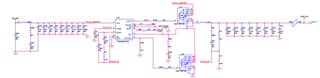
Here is the updated schematic.

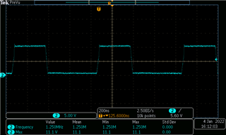
Below is the result of the EMI noise.

Let us know the workaround to resolve the issue.

  • Hi Pratik,

     Our US team will check it and reply you soon.

  •  

    From the frequency sweep that you presented, it looks like you're seeing excessive noise at 234MHz.  Typically elevated EMI noise in this frequency range is a result of noise radiating from the switching node during the rising and falling edge.  Parasitic inductance from the charge source - high frequency input voltage capacitors, to the switch-node capacitance resonates, causing the switching node to radiate high-frequency noise.

    Alternately, we could be seeing a resonance in the L-C filter that was added at the input due to insufficient damping.

    First, I would recommend checking the ringing frequency on the switching node of the TPS40305 controlled converter, and measuring the ringing frequency to see if this is the source.  If it is, we can focus efforts on reducing the ringing.

    I would recommend checking the layout of the switching node HDRV and BOOT nodes.  Avoid sharp 90 degree corners and unterminated traces on these high dV/dt nets selecting rounded for 45 degree chamfered corners.

    Avoid extending the switching node and Output voltage node under the inductor.  Bringing these nets close together under the inductor introduces high-frequency capacitance in parallel with the inductor, which conducts high-frequency noise directly to the output.

    Avoid filling under the inductor with ground unless  the area under the inductor is connected to the ground plane with multiple vias.  Filling under the inductor with ground that is not tightly coupled to the ground plane with multiple low-inductance vias can make that ground trace an antenna and conductive plate increasing the SW to VOUT capacitance by presenting a lower impedance between those nets than to ground.

    If it is not, then I would recommend checking the Input voltage after the added inductor to see if there is 234MHz noise from a resonance on the input side of the converter.

    There is a lot of high-frequency input capacitors - 100pF, 470pF, 1nF, 4.7nF.  It's unusual to see so many high-frequency input capacitors in the design.  Assuming their layout relative to the switching power-FETs is not introducing too much inductance, they should be helping suppress the switch node ringing, along with the 10-Ω HDRV resistor and 3.3-Ω BOOT resistor.

    You could review the sizing of the 3.3-Ω snubber resistor relative to the characteristic impedance of the switching-node L-C tank to see if the snubber could be resized for improved performance.

    Additionally, the Damping capacitor (56μF) on the input is a little small relative to the 80μF ceramic capacitance at the input.  Increasing the damping capacitor to 100μF could make the damping more effective.

    The only big jump in capacitance that could be leading to inter-capacitance resonance is the 100nF to 4.7nF jump.  Reducing the 4.7nF capacitor to 2.2nF to further spread that jump and reduce intern capacitance resonance might help.

    If you need to create an oscilloscope "sniffer" probe, you can connect the ground wire of an oscillscope probe it its probe-tip, and move the resulting loop around the converter to locate the source of the 234MHz noise radiating from the converter.

  • Any progress on this issue based on my earlier feedback?

  • ​​

    Peter: From the frequency sweep that you presented, it looks like you're seeing excessive noise at 234MHz.  Typically elevated EMI noise in this frequency range is a result of noise radiating from the switching node during the rising and falling edge.  Parasitic inductance from the charge source - high-frequency input voltage capacitors, to the switch-node capacitance resonates, causing the switching node to radiate high-frequency noise.

    Alternately, we could be seeing a resonance in the L-C filter that was added at the input due to insufficient damping.

    Pratik: Should I bypass/remove this L-C filter?

    Peter: First, I would recommend checking the ringing frequency on the switching node of the TPS40305 controlled converter and measuring the ringing frequency to see if this is the source.  If it is, we can focus efforts on reducing the ringing.

    Pratik: I Checked that and we didn't find any ringing. Here is the snapshot of the switching frequency.

    Peter: I would recommend checking the layout of the switching node HDRV and BOOT nodes.  Avoid sharp 90 degree corners and unterminated traces on these high dV/dt nets selecting rounded for 45 degree chamfered corners.

    Avoid extending the switching node and Output voltage node under the inductor.  Bringing these nets to close together under the inductor introduces high-frequency capacitance in parallel with the inductor, which conducts high-frequency noise directly to the output.

    Avoid filling under the inductor with the ground unless the area under the inductor is connected to the ground plane with multiple vias.  Filling under the inductor with ground that is not tightly coupled to the ground plane with multiple low-inductance vias can make that ground trace an antenna and conductive plate increasing the SW to VOUT capacitance by presenting a lower impedance between those nets than to ground.

    Pratik: Kindly visit the attached screenshot.

    Peter: If it is not, then I would recommend checking the Input voltage after the added inductor to see if there is 234MHz noise from resonance on the input side of the converter.

    There is a lot of high-frequency input capacitors - 100pF, 470pF, 1nF, 4.7nF.  It's unusual to see so many high-frequency input capacitors in the design.  Assuming their layout relative to the switching power-FETs is not introducing too much inductance, they should be helping suppress the switch node ringing, along with the 10-Ω HDRV resistor and 3.3-Ω BOOT resistor.

    You could review the sizing of the 3.3-Ω snubber resistor relative to the characteristic impedance of the switching-node L-C tank to see if the snubber could be resized for improved performance.

    Pratik: Are you suggesting changing the snubber resistor value.

    Additionally, the Damping capacitor (56μF) on the input is a little small relative to the 80μF ceramic capacitance at the input.  Increasing the damping capacitor to 100μF could make the damping more effective.

    Pratik: I will update the result.

    The only big jump in capacitance that could be leading to inter-capacitance resonance is the 100nF to 4.7nF jump.  Reducing the 4.7nF capacitor to 2.2nF to further spread that jump and reduce intern capacitance resonance might help.

    Pratik: Do I need to change both input and output capacitors?

    Peter: If you need to create an oscilloscope "sniffer" probe, you can connect the ground wire of an oscilloscope probe it its probe-tip, and move the resulting loop around the converter to locate the source of the 234MHz noise radiating from the converter.

    Pratik: Request you to provide a reference document for the same.

  • Pratik: Should I bypass/remove this L-C filter?

    You can try removing / bypassing the inductor to see if that eliminates the noise by removing the resonance, or you can look at improving the damping to maintain the filtering effect of the L-C filter, but reduce the resonance.  Eliminating the L-C filter could result in increased switching frequency noise on the input, so improving the damping of the L-C filter is likely the better option.

    Pratik: I Checked that and we didn't find any ringing. Here is the snapshot of the switching frequency.

    The Switching node looks really good, as does the layout.  The high-frequency bypassing capacitors and the snubber look like they're doing a good job, so the issue does not appear to be switch node ringing, so I think we should focus on the input L-C filter resonance.

    Pratik: Kindly visit the attached screenshot.

    The layout looks really good.

    Pratik: Are you suggesting changing the snubber resistor value.

    Based on the ringing, I don't think it's necessary.

    Pratik: Do I need to change both input and output capacitors?

    I would try increasing the input L-C filter damping, or bypassing the input inductor before trying to change capacitors.  The inter-capacitance resonance is a long-shot, but I was trying to suggest everything for you, so you would have a series of things to check for.

    Pratik: Request you to provide a reference document for the same.

    Here is a good tutorial about using near-field sniffer probes to debug EMI problems

    https://www.emcsociety.org/wp/wp-content/uploads/2012/11/Debugging-EMI-problems-with-an-Oscilloscope_June2014.pdf 

    Here is another

    https://studylib.net/doc/18617164/sniffer-probe-locates-sources-of-emi 

    I was trying to find a tutorial on making a simple sniffer probe using the ground lead of a passive oscilloscope probe, but I don't see one.  This article - http://emcesd.com/tt070199.htm shows a passive probe with it's ground lead shorted to the probe tip, and discusses how that enables the probe to pick-up EMI fields in a different context.

    Alternately, you can make a much smaller sniffer probe by wrapping some bare wire around the ground barrel, and then looping it to the probe tip.  These make-shift sniffer probes are obviously not as effective or accurate as sniffer probes available from most Oscilloscope manufacturers, but they can still be useful to find sources of radiated EMI.

  • Any additional progress on this issue?