A related question is a question created from another question. When the related question is created, it will be automatically linked to the original question.
If you have a related question, please click the "Ask a related question" button in the top right corner. The newly created question will be automatically linked to this question.
The Charge pump voltage VCAP-VS should be around 12.2V - 13.2V.
To understand why the charge pump voltage is not as per specification, can you please provide us below information,
Schematics
Test setup and conditions
Did the charge pump voltage measure 5.4 upon initial power up or is it after performing any tests? this is to understand if the LM7481-Q1 failed in the process of performing any tests.
Have you tried replacing the IC with a new one ? Did it work ?
Thanks for sharing the schematics. For me to completely review the schematics and provide comments please share the FET part number. Also are there decoupling caps close to the input of LM74810-Q1.
In slide number that you shared, the only difference between LM7480-Q1 working sequence and non-working sequence is the 26V - 'Vout-local' rail. I don't see any obvious reason why LM74810-Q1 should not work when powered from PSFB Converter. Do you have any more observations.
In the slide no. 3, the Gate voltage seems to be ramping up even before the input voltage started to ramp up. Are you switching the input power supply from 'DC Source 26V' to 'PSFB Converter' ?
Can you share the VCAP voltage voltage waveform as well during failure condition ?
1. FET part number : FDBL86561-F085. decoupling caps: Close to the pinA and pin VSNS? I removed the decoupling caps close to pin A and pin VSNS yesterday.
2. In the slide no. 3. Mainly the power of VOUT-LOCAL is provided by PSFB. Not provided by DC power supply.
3. VACP waveform will be provided to you tomorrow, do you need other waveforms?
4. UVLOF will lock the VACP voltage? How to check UVLO ?
5. I tried to pull the OV pin low and EN/UVLO high(VS voltage). Doesn't seem to help.
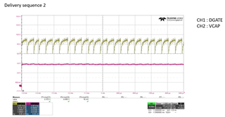
There is lot of switching on DGATE because of which the charge pump can be stressed. This can happen at no load or very light load condition or during AC rectification.
Are you testing at no load ? If yes, Can you please increase the load current to a level where the DGATE stops switching and then check the charge pump voltage ?
Is there ripple on input voltage ? The DGATE keeps switching if there is a voltage difference (enough to trigger Vsd(rev)) between input and output voltage.
Now the function is working properly. We have not modified the peripheral circuit, and we need to follow up on the issue to avoid recurrence.
Are you testing at no load ? If yes, Can you please increase the load current to a level where the DGATE stops switching and then check the charge pump voltage ?
=> No load test after loading DGATE on normal conduction
2.Is there ripple on input voltage ? The DGATE keeps switching if there is a voltage difference (enough to trigger Vsd(rev)) between input and output voltage.
Ca you please elaborate on my below two questions,
Are you testing at no load ? If yes, Can you please increase the load current to a level where the DGATE stops switching and then check the charge pump voltage ?
Is there ripple on input voltage ? The DGATE keeps switching if there is a voltage difference (enough to trigger Vsd(rev)) between input and output voltage.
Are you testing at no load ? If yes, Can you please increase the load current to a level where the DGATE stops switching and then check the charge pump voltage ?
==> Yes, no load. We have confirmed that the charge pump voltage is OK when we increase the load current to 10A.
2. Is there ripple on input voltage ? The DGATE keeps switching if there is a voltage difference (enough to trigger Vsd(rev)) between input and output voltage.