This thread has been locked.

If you have a related question, please click the "Ask a related question" button in the top right corner. The newly created question will be automatically linked to this question.

BQ76940: BATTERY MANAGEMENT SYSTEM FOR Li-ion BATTERY PACK

Part Number: BQ76940
Other Parts Discussed in Thread: BQ769200, BQ76200, BQ76920, BQ76930, BQ78350-R1A, BQ76952, BQ78350

I am designing a battery management system for a Li-ion battery pack for which I have shortlisted BQ76940 IC.

When I went over the Typical application schematic in the data sheet, there is a bidirectional MOSFET pair on the lowside. Also there is a P channel MOSFET at the gate of CHG MOSFET. Can you explain how these function? I have marked them in the schematic.
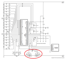
I also read that to drive the MOSFETs in the high side, we need to implement gate drivers. How important is this? The BMS will be managing a 48V, 60Ah battery.

Also the BQ769200 high side N channel FET driver doesn't seem to be available. Is there any alternative to it?

  • Hello Cleatus,

    Also there is a P channel MOSFET at the gate of CHG MOSFET. Can you explain how these function?
    This is explained in Figure 8. CHG and DSG FET Circuit of the datasheet. Basically, this is a low-cost PFET used to keep the CHG pin away from voltages below Vss.

    I also read that to drive the MOSFETs in the high side, we need to implement gate drivers. How important is this? The BQ769200 high side N channel FET driver doesn't seem to be available. Is there any alternative to it?
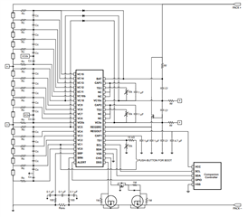
    It is necessary, driving high-side has different requirements than low-side. We do not have alternatives to the BQ769200 in our group. I do not know if TI has another FET driver that would directly work to achieve high-side with our part, you may have to look at TI's FET drivers catalog and see if any would fit.

    I apologize for the stock situation.

    Best Regards,

    Luis Hernandez Salomon

  • How do the bidirectional MOSFET pair on the lowside work?

  • Hello Cleatus,

    Albeit for a different part, the explanation described in Section 1 of the Using Low-Side FETs with the BQ76952 Battery Monitor Family application report should be useful in understanding how the low-side MOSFET pair work.

    See Section 8.5 Electrical Characteristics — CHARGE AND DISCHARGE DRIVERS in the datasheet for the drive behavior using the BQ76940.

    Hope this was useful!

    Best Regards,

    Luis Hernandez Salomon

  • Thank you for your answer! I have some more questions.

    I am designing a battery management system for an Automated Guided Vehicle. Should I go for low side MOSFET pair or high side MOSFET pair? Which configuration is the most advantageous?

    Can I implement both high side and low side MOSFET pairs at the same time?

  • Hello Cleatus,

    This depends on many factors and ultimately depends on the system's requirements and standards needed. If your application requires high/low, use whichever it is required. The BQ76940 has integrated low-side drive, for high-side driving, a FET driver like the BQ76200 might be needed. 

    This is a common question and this older e2e thread may help resolve your question: 

    https://e2e.ti.com/support/power-management-group/power-management/f/power-management-forum/784837/bq76920-low-side-switching-or-high-side-switching-which-one-should-prefer-and-why

    Best Regards,

    Luis Hernandez Salomon

  • Thank you very much for your valuable inputs so far!

    Can you suggest an alternative to BQ76200 high side gate driver?

  • Hello Cleatus,

    This is the only high-side gate driver we have in our group. We do not have an equivalent part in the battery product line.

    You could look into other FET driver products that TI offers and see if there is one that will meet your needs: 

    https://www.ti.com/power-management/gate-drivers/products.html

    Best Regards,

    Luis Hernandez Salomon

  • Can I implement pre charge function if using low side MOSFETs?

  • Hello Cleatus,

    It is possible to implement pre-charge using low-side. See this older e2e thread for some guidence:

    https://e2e.ti.com/support/power-management-group/power-management/f/power-management-forum/488965/how-precharging-function-is-working-in-bq76940

    Best Regards,

    Luis Hernandez Salomon

  • What is the maximum cell balancing current per cell for internal balancing? In absolute maximum ratings table it is mentioned as 5 mA but in section "10.3.1.3.3 Cell Balancing", it is mentioned as 50 mA.

  • Hello Cleatus,

    This 50-mA balancing current per cell is for the BQ76920 part. The BQ76930 and BQ76940 parts both can balance up-to 5-mA per cell, which is why external cell balancing is recommended for these parts.

    See Section 4 of the bq769x0 Family Top 10 Design Considerations application report for a detailed description of the cell balancing operation using this part.

    Best Regards,

    Luis Hernandez Salomon

  • I have prepared a circuit based on the typical applications schematic as shown in the data sheet with 9 cells interfaced to BQ76940. I tried powering ON the circuit without the microcontroller interfaced and noted approximately 33V between PACK + and PACK -. I connected both the terminals to an electrical load bank which was set to draw 0.5 Amps but there was no current flowing to the load bank. The gate voltage from CHG and DSG pins were approximately 0.5V. Won't the IC allow charging or discharging without the microcontroller or should I enable the ADC using the microcontroller first? 

  • Hello Cleatus,

    Yes, you need the microcontroller to enable the FETs. You need either a microcontroller or the BQ78350-R1A companion gauge in order for the BQ76940 AFE to function properly. It is not able to work standalone.

    This is the first question (1.1 Can I use the part as a standalone protector?) of the bq76920, bq76930, bq76940 AFE FAQ, which may be useful for some of the questions you may have about the part.

    The newer BQ76952 is able to work standalone, without a MCU. However we are facing stock issues, so it is not an easy part to obtain.

    I hope this helped. If you have any further questions, let us know!

    Best Regards,

    Luis Hernandez Salomon

  • When I measure the voltage across PACK+ and PACK-, I get a reading of approximately 5V. Is it normal? I have not connected the microcontroller yet.

  • Hello Cleatus,

    When you measure across PACK+ and PACK-, PACK- should be floating if both FETs are off. So not entirely sure where this would be coming from.

    There is no ground point of reference when measuring like this. Since both FETs are off and disconnected from Vss.

    Best Regards,

    Luis Hernandez Salomon

  • Thanks for your help so far Mr. Luis!

    I have few more questions:

    1. PIN 7 (CAP1) and PIN 3 (VSS) show a short when checked for continuity between them. Does it mean the IC is damaged? But PIN 20 (BAT) and PIN 3 (VSS) don't have continuity between them.

    2. Can I continue testing with the IC despite the short (in accordance to point 1)?

    3. The voltage from PIN 8 (REGOUT) is 0V despite PIN 9 (REGSRC) receiving a 9V (measured between REGSRC and VSS). Should it output any voltage when powered ON as a standalone unit without a microcontroller interfaced?

  • Hello Cleatus,

    No problem! Glad to help Slight smile

    1. PIN 7 (CAP1) and PIN 3 (VSS) show a short when checked for continuity between them. Does it mean the IC is damaged? But PIN 20 (BAT) and PIN 3 (VSS) don't have continuity between them.
    For CAP1, you should have a capacitor here to Vss, and once you boot the IC (by using TS1) the CAP1 voltage should be ~3.3-V. If the part is shutdown (or no capacitor is there), then I believe it is possible that CAP1 is shorted to Vss. It's also possible the part could be damaged.

    2. Can I continue testing with the IC despite the short (in accordance to point 1)?
    You want to measure CAP1 to be ~3.3-V before continuing testing. Not having a voltage there implies the part is in shutdown or could possibly be damaged.

    3. The voltage from PIN 8 (REGOUT) is 0V despite PIN 9 (REGSRC) receiving a 9V (measured between REGSRC and VSS). Should it output any voltage when powered ON as a standalone unit without a microcontroller interfaced?
    At 9-V supplied, I believe it should still work. You should be getting either 2.5-V or 3.3-V (depending on part number) at REGOUT. It could be that the part is off (from the previous questions). It may be useful to read Section 9 REGSRC Supply of the bq769x0 Family Top 10 Design Considerations application report. Which explains in more detail REGSRC considerations to power the LDO. 

    Best Regards,

    Luis Hernandez Salomon

  • I have changed the IC with a new one. Now, I'm getting the following readings:

    CAP1-VSS = 3.29V

    CAP2-VSS = 14.6V

    CAP3-VSS = 25.8V

    REGOUT-VSS = 3.3V

    CHG-VSS = 0V

    DSG-VSS = 0V

    1. Are these values fine?

    2. When I check the voltage across PACK+ and PACK-, I'm getting 28V. How is this possible when both the MOSFETs are switched OFF.

    3. Can you suggest a high side gate driver for BQ76940? I'm not able to find a suitable driver.

  • Hello Cleatus,

    1. Are these values fine?
    Yes, the values seem okay. For the CHG/DSG FETs, make sure you are measuring the gate-source voltage to see exactly at what state it is. However, it should be okay.

    2. When I check the voltage across PACK+ and PACK-, I'm getting 28V. How is this possible when both the MOSFETs are switched OFF.
    I am not sure, if both FETs are off then measuring PACK+ would be left floating. Could it be that there is something grounding the PACK- trace to Vss? 

    3. Can you suggest a high side gate driver for BQ76940? I'm not able to find a suitable driver.
    The BQ76200 is the high-side gate driver that we usually recommend and is the only gate driver we have in our product line. If this is not suitable due to stock issues or other things, then you may have to ask for advice to the FET gate drivers group.

    If you are not using the BQ78350 or an MCU, you can evaluate the BQ76940 using the bq769X0 Evaluation Software found in the product page of the device, which may be helpful in debugging some issues.

    Best Regards,

    Luis Hernandez Salomon

  • I have few more questions.

    1. The maximum current that can be drawn from the REGOUT pin is 45mA. Am I correct?

    2. How is the value of current sense resistor chosen? Are there any calculations for it?

    3. Can I use the same IC to balance and monitor cells in parallel?

  • Hello Cleatus,

    1. The maximum current that can be drawn from the REGOUT pin is 45mA. Am I correct?
    Yes that's correct.

    2. How is the value of current sense resistor chosen? Are there any calculations for it?
    The sense resistor is chosen to maximize the Coulomb Counter ADC of +/-200-mV. Read Section 11.2.2.1 Step-by-Step Design Procedure of the datasheet.

    3. Can I use the same IC to balance and monitor cells in parallel?
    No, you would not be able to balance/monitors cell in parallel. There's no good way to do this as the IC only is able to measure the voltage of the cells, so any parallel cells would show as a single voltage to the IC.

    Best Regards,

    Luis Hernandez Salomon

  • Hey Luis! I have couple more questions.

    1. I will be using an external balancing method. How can I determine the balancing current rate?

    2. I have attached my schematics that I have designed. It will be a development board with both high side and low side configurations for testing purposes. Can you provide your feedback on the same if possible?

    cell_conn.pdffuel_gauge.pdfmosfet_cfg.pdf

  • Hello Cleatus,

    1. I will be using an external balancing method. How can I determine the balancing current rate?
    The balancing will be determined by the external balancing resistor (the resistance in the external FET path). See Section 4 Cell Balance of the bq769x0 Family Top 10 Design Considerations application report to see the current path during external cell balancing.

    2. I have attached my schematics that I have designed. It will be a development board with both high side and low side configurations for testing purposes. Can you provide your feedback on the same if possible?
    For the high-side pre-charging resistor. Is 1-MOhm appropiate for your application? This would be a very low charging current. See Section 8.1.1.4 Precharge and Predischarge Support of the BQ76200 datasheet. It may be good to add the capacitor couple seen in C40/C41 across the Q25/Q26 high-side FETs. I'd also recommend add a Zener diode across the gate-source of each gate to protect the FETs in case of a high transient.

    The VDDCP capacitor can be smaller as you are only using 2 FETs, see Section 6 VDDCP Capacitance Reference Table of the FET Configurations for the bq76200 application report. The larger the capacitor, the slower the start-up time will be.

    You also want to add a 100-Ohm gate resistance to the FETs of the high-side circuit. I'd recommend you read the bq76200 Beyond the Simple Application Schematic report which discusses this topic and other topics on the BQ76200 design. A Zener and resistor may be added between the PACK and DSG pins of the BQ76200 can be used to avoid excess voltage between the pins during DSG turn on and avoid internal switching losses, this is also mentioned and shown in Figure 12 of the previous application report.

    Everything else seems okay from what I can see. If you have any questions/concerns let me know.

    Best Regards,

    Luis Hernandez Salomon

  • Cleatus,

    A couple of comments from another member of the team regarding your schematic:

    • R69/R70/R71 should be 1-kOhm ideally.
    • Although the 0.1-uF capacitance of C1-C18 is okay, 0.22-uF may give better voltage measurement accuracy during cell balancing because of lower RC time constant.

    They thought everything else seemed okay.

    Best Regards,

    Luis Hernandez Salomon

  • Thank you Luis! I have made the necessary changes to my design.

    I have another query. How does the BMS react to Constant Current and Constant Voltage while charging?

  • Hello Cleatus,

    Glad to hear that! Also, just noticed I made a typo with the second bullet point, I meant to say 1-uF instead of 0.1-uF.

    The IC would have no issues if there's a constant current/voltage during charging if it is within normal condition parameters to not trigger any faults. For the specifics of the charger itself, you would have to open a new thread to ask the charger team.

    Best of luck! Slight smile

    Best Regards,

    Luis Hernandez Salomon

  • Thank you Luis!

    How can I implement simultaneous charging and discharging using this IC?

  • Hello Cleatus! 

    This depends on the charger current. I believe this question may be better suited for the charger team.

    Technically you cannot charge/discharge a battery at the same time with any BMS, however, the charging current can be enough to keep the load running if needed, if the current isn't sufficient, then the battery would supply the additional current needed.

    For example, if a load is drawing 5 Amps, and the charger supplies 3 Amps, then the battery would supply 2 Amps.

    In the case where the charger were to supply 6 Amps, then the load would draw 5 Amps and the battery could be charged at 1 Amp (while also keeping the load powered)

    In either case, the battery itself is never charged or discharged at the same time. So there's no need to change the circuitry of this IC.

    Best Regards,

    Luis Hernandez Salomon