This thread has been locked.

If you have a related question, please click the "Ask a related question" button in the top right corner. The newly created question will be automatically linked to this question.

TPS54620: Device not working, oscillation and high current drain

Part Number: TPS54620

Hello,

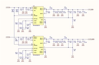
I've designed a system with two TPS54620, supplied by 12V.

The first device shoulde provide 5V output and the second one 2V5 output. The second device is enabled by the Power Good of the first.

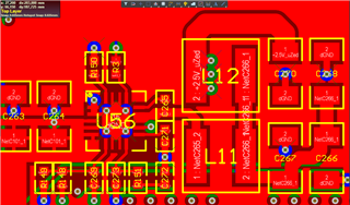
You can see the complete schematic attached. DNM resistors are not mounted into the board.

There is a problem, the first device doesn't work, when I power on the board I hear a strong noise from the chip and there is a high current drain from power supply, very high (more then 500 mA, limited by the supply) with no load. I think the noise is an oscillation, but I don't explain the current drain with no load. I can't complete any measure with such level of current drain that could damage the chip or the board.

The second device is not enabled because the first doesn't work properly and there is no way to test it, without removing (destroying) the device, that is actually unavailable.

Please can you help me to fix the problem?

I don't see big mistakes on the schematic and the PCB is ok.

  • Hello Marco,

    I can not see your schematic as the link is blocked by TI site.

    Can you attach the schematic instead of a link?

    Regards,

    Yitzhak Bolurian

  • Hello again,

    It is also recommended to increase the input voltage gradually, starting at Vin=0, and check at which point it starts to draw high current (500 mA).
    Please try this and advise.

    Regards,

    Yitzhak Bolurian

  • Hi Marco,

    Nothing obvious is wrong with the schematic.

    Your soft start time is set to about 8mS, so your Cout charging current should be only 1/8 Amps.

    Please try to raise the input voltage slowly and see what voltage level triggers the high current consumption. 

    Regards,

    Yitzhak Bolurian

  • Thanks, I'll try, but do you think noise from chip (maybe oscillations?) and high current consumption are related?

  • Hi Marco,

    We have no evidence of that yet. 

    Let's try the gradual increase in Vin first.

    Regards,

    Yitzhak

  • Hello,

    from 0 to 4.5V: no chip noise and no current comsumption

    At 5V noise start and current consumption is about 50 mA with no load

    At 6V noise is stronger and current consumption becomes very high (more than 100 mA) with no load.

    Noise change frequency with input voltage.

  • Hello Marco,

    Now we know that the circuit draws high current only after switching gets started.
    You may be right, this could be caused by stability issues and oscillation.

    You are having a two stage output filter on both stages.
    That can lead to a lot of phase shift that may lead to stability issues.
    As the first debugging step, I would suggest that you by pass L10 and L12 with short circuit/wires in parallel to those and see if the oscillation is gone.

    Regards,

    Yitzhak

  • Hello, 

    I removed L10 and replaced it with a 0 ohm resistor. The problem is still here, noise and high current consumption starting from 5 V.

    We could try to change switching frequency to a lower/higher value and see what happens. Or we could change the compensation network to lower the compensation pole. R147 takes a role in that network and is easy to change.

    What do you think about? I have no more idea, please give me some other debug steps.

    Regards

  • Hello Marco,

    Yes, changing the compensation seems to be the next step to stabilize the loop.
    Please give this a try.

    Regards,

    Yitzhak

  • Hello, I'll try as soon as possible.

    A lower frequency compensation pole and zero should be desidered, right?

  • Hi Marco,

    Yitzhak will check it and reply you soon.

  • Hi Marco,

    Not necessarily.
    A quick try can be to just remove the feed-forward-cap ( C258), you may get a stable loop just by removing the cap.
    This cap pushes the cross over frequency too high and cause instability.

    In case the above does not help then, you could use the attached calculator tool or WeBench to design your compensation.
    But before you do that, you have to know how much derating of the output capacitor values you can expect at 5V.
    The derating varies based on the capacitor type and voltage rating.

    7128.SWIFT_PeakCMC_Calculator_RevA.xlsm

    The WeBench tool at at the bottom of this page:

    https://www.ti.com/product/TPS54620

    Hope this helps.

    Regards,

    Yitzhak Bolurian

  • Hi,

    removing that cap helps a bit, I mean the chip is stable for 1-2 seconds after power on than starts to oscillate, but with less current consumption.

    Finally I can meaure voltage on the output, so this is a nice improvement, 5V and 2.5V are there but unstable.

    I noted that only the first device U55 make noise, while U56 not. Maybe only U55 is unstable, and the oscillations propagates on the output of the second device. I don't know why, anyway I'll play a bit with compensation network.

    Thanks, 

    regards.

  • Hi Marco,

    Please share your test progress when you got any updates.

    For now, I will close this thread.

  • Hi Marco,

    Glad that we have progress.

    You should be able to stabilize the loop with the provided tools.

    Let me know if further help is required.

    Regards,

    Yitzhak

  • Hello,

    the loop is still unstable, I changed the passive components according to the tool, with a good phase margin, but still noise, oscillations and current consumption. The noise comes always for the first chip U55 but not from the other one.

    I used 470pF for C262, 1K for R147 and 100 nF for C261 with no luck. 

    I don't know to do, really a strange situation, maybe a defective chip?

    This is my only opinion at the moment, however is not available on the market actually, so is difficult to change and try.

  • Hello Marco,

    So the second stage is working and stable now?

    If so, can you swap between the two ICs?

    You can order a TPS54620EVM-374 EVM and run your stability test or swap between the ICs as well. I have checked and it seems to be available.

    Regards,

    Yitzhak

  • No, the second stage is not stable, that chip doesn't make audible noise but I see oscillations with the scope.

    I don't know if it's unstable itself or the oscillations of the first stage propagate to the output of the second.

    It's not so easy to swap between the two ICs, without to damage them during desoldering process.

  • Hello Marco,

    You should disconnect the EN of the second stage from the PWRGD of the first stage before you check the second stage.

    Also the new compensation values that you have selected are a bit atypical, and set the Fco frequency to less than 2 KHz!

    More typical compensation values could be, 4.7pF for C262, 41.2K for R147 and 5.6 nF for C261 and 27 pF for C258.

    Sorry that I can not help you with the IC availability.

    Regards,

    Yitzhak

  • Hello,

    just a summary of the situation: actually I removed U55, so only U56 is mounted on PCB.

    Now U56 is making noise, so there is a common problem to both stage, a design issue, this is the first evidence.

    I can observe 1 V p-p oscillation at 10 kHz on the output of U56 that should be 2.5V. Is a perfect sinewave centered at 3 V with that audible frequency.

    Current consumption with no load is about 200 mA (abnormal). Compensation value: R151=6.34 K, C272=100nF, C273=68pF, C269=not mounted

    According to the tool and datasheet they are good values, so the loop should be stable.

    With a higher switching frequency same problem and IC draw more current (300 mA) with no load.

    There is a design issue somewhere and I don't find it, is an important university project I have to solve it.

    Here a picture of the PCB. I don't see any big mistake, could be better of course.

  • Hello Marco,

    Regarding the layout, why the GND2 and GND3 pins in the layout are not connected on the top layer to the dGND ground plane?
    The plane is just to the left side of the pins!

    Those GND pins better be connected to dGND directly at the top layer, and not through vias.

    Please look at the Vin signal on the pins of the device (Between VIN/PVIN and the adjacent GND pins), and see if the input voltage arriving at the device is clean.

    Also EN pin on TPS54620 has a 6V max rating and should not be pulled high all the way to VIN of 12V. You will need a voltage divider there.
    Please look at these two issues and get back with the results.

    Regards,

    Yitzhak Bolurian

  • Hi Marco,

    Have you had the chance to look into these comments/recommendations?

    Regards,

    Yitzhak Bolurian

  • Hello, sorry for the late, I've been busy with other jobs.

    In the top layer there is a different GND plane, it's isolate from dGND of the TPS converter, so I have to use vias.

    The input voltage is absolute clean. Yes, I know the max value for EN is 6 V, but in the design is floating, there isn't a pull up to VIN.

    I can't still understand why it doesn't work.

  • Hello Marco,

    What do you mean by "different GND plane"?
    If you look at the recommended layout examples by TI in the data sheet and the EVM's user guide you can see that TI recommends these GND pins to be connected to a ground plane at the same/top layer and not through vias. vias add extra inductance and are not as effective in grounding at high frequencies.

    You may need to replace the device. It might be damaged.

    Regards,
    Yitzhak