- Ask a related questionWhat is a related question?A related question is a question created from another question. When the related question is created, it will be automatically linked to the original question.
This thread has been locked.
If you have a related question, please click the "Ask a related question" button in the top right corner. The newly created question will be automatically linked to this question.
Hello,
I'm facing some issues when designing a board using these DC/DC converters. Both of the issues are related to the PG signal:
I'll kindly ask for someone to shed some light on this issues.
Thanks!
Hello Francisco,
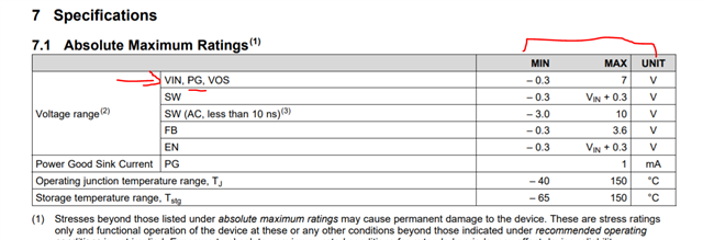
PG can also be pulled up to system rail with a pull up resistor but by making sure that the PG pin rating mentioned in the datasheet has not exceeded.

The PG pin behavior of TLV62084A is also explained in detail in this application note: https://www.ti.com/lit/an/slva803/slva803.pdf
I hope it can help you more in understanding it better.
Also please remember that there is a difference between PG pin behavior of TLV62084 and TV62084A. (Table 2 and Table 3 in D/S).
2) Coming to your second point, yes you are right VPG is voltage that you get the PG pin with a pull up resistor. So if you have a look at below graph, there is a time when Vout is rising or during the softstart delay before Vout starts to rise, PG pin is low for TLV62084A there (VPG<=VFB) will be valid

I hope it clears your points.
Thanks and Best Regards,
Farheen
Thanks for your help @Farheen.
I haven't seen the application note before, and helps to understand the PG behaviour.