This thread has been locked.

If you have a related question, please click the "Ask a related question" button in the top right corner. The newly created question will be automatically linked to this question.

BQ76952: Question about ESD protection

Part Number: BQ76952
Other Parts Discussed in Thread: , BQ76942

Hi

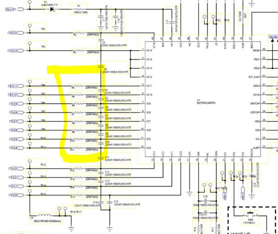
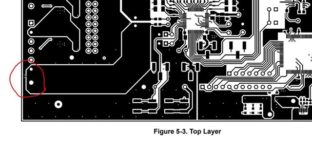
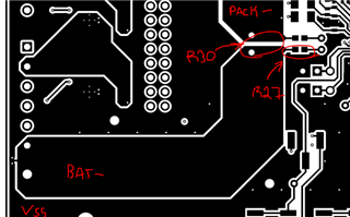
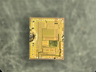
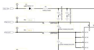
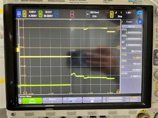
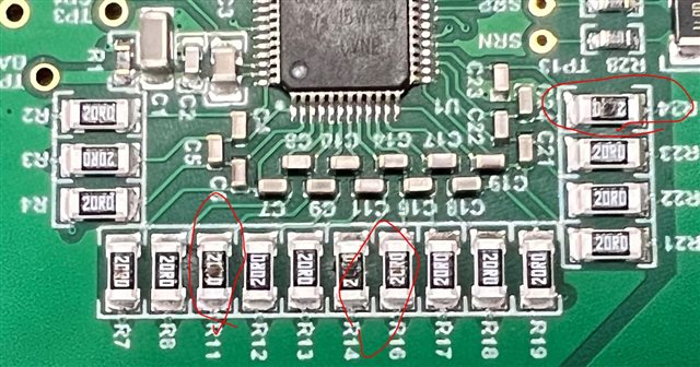
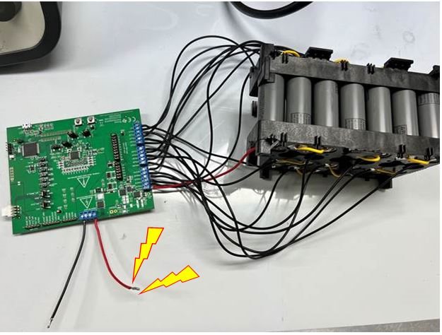
It is said that my customer keeps failing in the esd test.

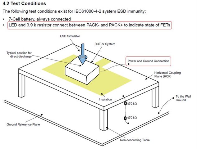
ESD : Contact ±8~10KV

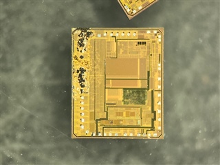
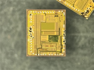
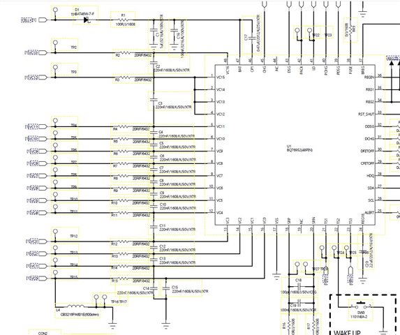
Fail point: bq76952 or 

Is there anything to guide about? For example, PCB correction, circuit correction, etc..
Let me know if you have any related information.

Thanks

  • Hello David,

    A couple of questions about your ESD test: 

    • How is your ESD test being conducted? 
    • How is the part failing? What failure is being shown from the BQ76952? Does the part reset/break?

    Albeit different parts are mentioned in these, there's been a couple of questions on ESD these past couple of days that may be useful as the ESD protection is very similar to the BQ76952:

    https://e2e.ti.com/support/power-management-group/power-management/f/power-management-forum/1070344/bq76940-smbus-and-i2c-esd-protection

    https://e2e.ti.com/support/power-management-group/power-management/f/power-management-forum/1070739/in-the-electrostatic-test-with-6kv-or-8kv-air-discharge-hit-b0-or-b15-chip-will-stop-working-mcu-reset-once-again-normal

    In addition to these, we do have an ESD Stress Test Report with the BQ76952, which may be helpful.

    Best Regards,

    Luis Hernandez Salomon

  • Hi

    Refer to below.

    • How is your ESD test being conducted? 
    • =>ESD Contact ±8~10KV
    • How is the part failing? What failure is being shown from the BQ76952? Does the part reset/break?
    • =>Yellow resistance dies or IC dies  in the circuit diagram below.
    • Thanks
  • Hello David,

    Do you have any ESD protection components in your design?

    Best Regards,

    Luis Hernandez Salomon

  • Hi Luis

    There is no ESD protection components.

    Thanks

  • Hello David,

    Where are the ESD contact tests done?

    I'd recommend you still read the last reply in the following thread: https://e2e.ti.com/support/power-management-group/power-management/f/power-management-forum/1070739/in-the-electrostatic-test-with-6kv-or-8kv-air-discharge-hit-b0-or-b15-chip-will-stop-working-mcu-reset-once-again-normal

    It has some comments about ESD protection. It also points to SLUA368, which is an application report that explains ESD considerations for the BQ20Zxx family, however, the principles are the same for our device, so it is a great resource to read.

    In the EVM for the BQ76952 we added spark gaps and ESD  capacitors in the PACK+ path for ESD protection. In addition a TVS diode and spark gap was also added in each of the communication lines to protect the pins against ESD. 

    I'd recommend you add some components to protect against ESD if needed and to read the post/application report to see if these considerations were taken in mind when designing your board layout. 

    If you have any particular question let us know

    Best Regards,

    Luis Hernandez Salomon

  • Hi Luis

    Please refer to the attached file.

    The customer wants to know how to do GND when testing ESD.

    The current condition is that P+ of BMS is not grounded and the ESD gun is grounded.

    ESD TEST Condition.pptx

    Thanks

  • Hello David,

    It may be useful to test the ESD at lower voltages, and slowly go up to see where it fails.

    It may also be useful to see our BQ76952EVM Board files, this can be found under the Design files section of the BQ76952EVM page. It includes the schematic and board layout. We've stress tested our EVM for ESD, which you can see in the ESD Stress Test Report with the BQ76952. In our tests, we made ESD contacts on PACK+, PACK-, SDA, SCL with voltages up-to 25-kV. It passed all tests.

    What is the purpose of the inductor to Vss? We are concerned this may have some unintended issues with the grounding path. It seems that this is what is connecting the bottom cell to Vss. Ideally you would want the high current path to flow from the bottom cell (BAT-) to the sense resistor. Once again, see our EVM files for an example. You can also see the BQ76952EVM User Guide for images of the layout.

    I cannot see your whole schematic, but I am not sure if you have the ESD capacitors or spark-gap in your design or any other ESD protection components in your device. These could help. In addition you may want to add TVS diodes for additional ESD protection if it's still of concern afterwards. Sharing the schematic may be helpful to see if you have these.

    Something you could try to see if the grounding/current path is the main issue, is to place a cable from the bottom cell's negative connector (BAT-/VC0) to the sense resistor, and conduct the ESD test again. The way you debug this will ultimately be up to you. If further issues still arise, you may have to further evaluate your design and modify it accordingly.

    Best Regards,

    Luis Hernandez Salomon 

  • Hi Luis

    Thanks for your support.

    I have an additional question.

    Looking at the user guide of BQ76952EVM, R27 and BAT- are connected by thin lines.

    <Image= p.26 of BQ76952EVM page>

    Is it right that only thin lines are connected?

    Can this affect ESD?

    Thanks

  • Hello David,

    No, this is the net-tie that connects BAT- to Vss. This keeps most of the high-current contained in the BAT-/PACK- path, yet still keeps BAT- as the Vss reference.

    Here's a picture that may help:

    This is to help avoid the higher currents to reach the IC and affect it. It can have an impact on ESD protection. It is mentioned in Section 4 of SLUA368 to keep the IC separate from the high-current pathway.

    Best Regards,

    Luis Hernandez Salomon

  • Hello. luis
    Regarding the ESD TEST problem, we requested continuous improvement through David.
    However, there is no improvement, so please inquire.
    After ESD test, there is burnt in cell balansing part. In this regard, I ask the following questions:

    Q&A
    1. Why is only the cell balansing part damaged in a specific location?
    2. Why is there no damage to the positions of Pins 1 to 4 on the circuit diagram above?
    3. Even if you remove the parts around the FET and connect only the cell power, the IC will be damaged.

  • Hello,

    Resolving ESD issues can be difficult since conditions can be very different for each layout design.

    I am not sure why these were damaged this way. What were the damaged pins exactly? 

    Look into the documents I shared before and in our EVM board layout. We keep the IC away from the high-current path, during an ESD event you would want most of the current to flow away from the IC and through the high current path between the pack pins and into the battery cells, as voltage remains constant between the cells. 

    I see from the layout images that there may be some ESD components between the PACK+/PACK- pins, what exactly are these? If needed, you may want to add additional ESD components at these connections.

    Best Regards,

    Luis Hernandez Salomon

  • Hi Luis

    Thanks for your support.

    Please refer to below.

    -Waveform-

    Ch.1: TP3 in SCH

    Ch.2:TP2 in SCH

    Looking at the waveform of the oscilloscope, the voltage rises to about 20V as soon as the ESD is applied.

    Question: Does bq76952 recognize this voltage as a battery voltage and perform cell balancing when it goes up to 20V?

    I wonder if cell balancing is activated when the voltage rises due to ESD.

    Thanks

  • Hello David,

    Cell balancing would occur due to the differential voltage, what is the differential voltage of the cells? In addition, at default it should only balance when there is a charge current.

    I am a bit concerned as to why it increases 20-V for what seems a few seconds after ESD. Is the IC damaged at this point?

    Best Regards,

    Luis Hernandez Salomon

  • Hi Luis

    Is the IC damaged at this point?

    => Yes

    Is it wrong to go up to 20V because of ESD?

    Thanks

  • Hello David,

    Yes, this is not a normal behavior. From a quick glance at the layout from your original post, it doesn't seem like there is a defined high-current path for the IC, as I mentioned was important in my previous comments. In our EVM we connect BAT- to Vss through the net-tie in order to keep the high-current path separate from the IC path. Correct me if I am wrong, but it seems that the sense resistor is connected to B-, which is spread all over the PCB layout? So the high-current path could reach unintended locations. 

    This might not be the exact cause, but it could be something to look at. Look at the documents I provided and EVM layout for reference.

    You may need to hire an external ESD consultant that may be able to provide guidance on the layout for ESD protection, as ESD failures can be difficult to debug and may need careful layout considerations in your design that we may not be able to help. 

    I can keep this thread open if you have any further questions.

    Best Regards,

    Luis Hernandez Salomon

  • Hi Luis

    BQ76952EVM was provided and the ESD test was conducted.

    However, it failed as shown in the picture.

    Test condition : Contact +8kV 

    So I think my test method is wrong.

    As shown in the picture, only 16s1p cells were connected and tested. (ESD Point: Lightning sign)

    Did we do anything wrong?

    Can you tell me how to do your ESD test?

    Thanks

  • Hello David,

    We show the set-up for the test in Section 4.4 Test Setup of the ESD Stress Test Report

    Best Regards,

    Luis Hernandez Salomon

  • Hi Luis

    My customer reviews the data you sent and asks you.

    1. Connect 3.9k resistor between pack+ and pack- and test it?

    2. Can you tell me more about Power and Ground Connection?
        For example, how to connect the ESD gun and the GND.

    Thanks

  • Hi David,

    I did the testing for this device both on the EVM and on the 2-layer board that more closely resembled a real application. The 3.9k resistor and LED were installed between the PACK+ and PACK- pins to monitor whether the FETs were turned off at any point (due to a protection triggering or a reset of the device). The device registers were first configured for the number of cells connected and the FET_ENABLE() command was sent to enable the FETs. At that point the PC was disconnected from the EVM to do the IEC ESD testing.

    I am not sure what could be causing the damage to the board and to the device that you are observing. The one big difference I notice is that you have some very long wires connecting the battery cells to the board and on the PACK+ / PACK- pins. I do not know if these could be major factors.

    http://www.noiseken.com/uploads/photos0/240.pdf 

    https://transientspecialists.com/blogs/blog/esd-testing-equipment-methods-standards-air-contact-discharge

    Regards,

    Matt

  • Hi Matt

    Below is the ESD test result of bq76942 you told me.

    https://www.ti.com/lit/an/sluaa15/sluaa15.pdf?ts=1646720673520

    Do you have the results of the ESD test for bq76952?

    Thanks

  • Hi David,

    The BQ76952 was tested at the same time as the BQ76942. Our IEC ESD testing lab does not permit DC voltages above 50V for safety, so a 7S battery (with BQ76942) was used for the report. However, many customers have gone through IEC ESD testing with larger batteries with the BQ76952 and have had good results. 

    I am still puzzled why the damage occurred on the EVM because I also did extensive testing on the EVM without ever seeing damage. I notice from your picture that you have all of the cell simulator (resistor divider) jumpers installed, so you are connecting a battery and a resistor divider. You should not connect both. As I mentioned before, your wires are very long. The EVM does have components to help with ESD protection. Did you communicate with the EVM first before applying the ESD voltage to make sure the device was powered up and working? Did you enable the FETs by sending the FET_ENABLE() command?

    Regards,

    Matt

  • Hi Matt

    Thanks for your support.

    I don't know what  cell simulator (resistor divider) is like.

    Could you explain it to me? 

    Thanks

  • Hello David,

    A cell simulator is used with a power supply in order to simulate a cell voltage that the IC can measure. 

    Read Section 4.1 Cell Simulator of the BQ76952EVM User Guide.

    You need to remove the shunts of the J14 and J23 headers in order to disable the resistor divider. 

    After you remove these and follow the recommendations by Matt, do you still see an issue after ESD testing the EVM?

    Best Regards,

    Luis Hernandez Salomon

  • Hi Luis

    When I changed the cell and tested it, I passed the ESD test.

    Before: INR21700M 50LT https://www.batteryspace.com/prod-specs/11514.pdf

    After: INR18650 MH1 https://www.tme.eu/Document/21ae98ff53f5d39fe5ebfe42dfc0a574/INR18650MH1.pdf

    Does the cell capacity affect the ESD test?

    Which cell did you take the ESD test?

    Thanks

  • Hello David,

    That is very interesting. I don't believe that cell capacity should affect the ESD test. But I will ask the team and see what their thoughts are.

    If you conduct the ESD test, do you see a change in the battery voltage during the test?

    Best Regards,

    Luis Hernandez Salomon