This thread has been locked.

If you have a related question, please click the "Ask a related question" button in the top right corner. The newly created question will be automatically linked to this question.

TPS40210-Q1: The trouble with MOSFET heating

Expert 1025 points
Part Number: TPS40210-Q1
Other Parts Discussed in Thread: TPS40210

HI,

   Recently, when debugging tps40210, it was found that the MOSFET was seriously hot, and the temperature rose to about 80°C (Vin=12V, Vout=90V, no load). All the resistance and capacitance parameters are calculated according to the webbench power designer. Can anyone help analyze what the problem is?

Attached are schematics and PCB files

01_HV supply.pdf

driver.PcbDoc

  • Hi Suy,

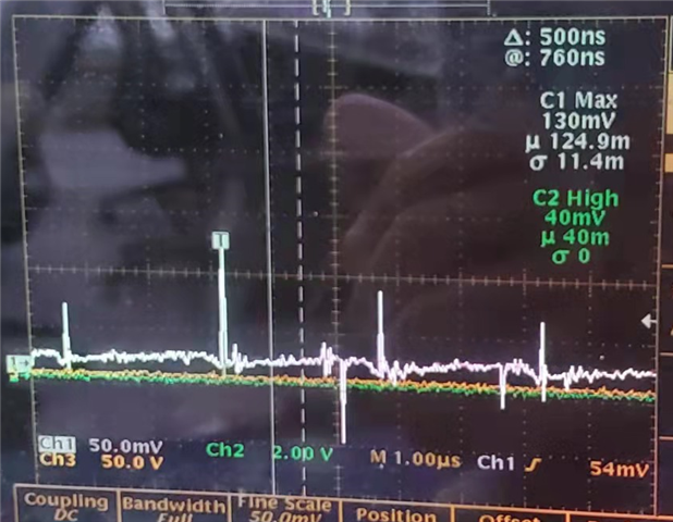
    Can you please try to measure the Switch node (L1/D1/Q1 connection point) , Gate of the FET and the voltage on R8 in this condition and send the scope picture.

    Note: haveing 100V rated output Capacitors for an 90V output is very close to the margin. For the cap i suggest to have at least 40% margin on the voltage to ensure save operation with temperature and aging considered.

    Best regards,

     Stefan

  • Hi Stefan,

         Thanks for your reply!

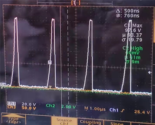
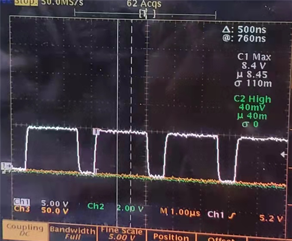
         The following is the switching node, gate of MOSFET,the voltage on R8 :


  • Hi Suy,

    it looks like the switch off of the FET is quite slow. This could lead to a higher power dissipation during this switching phase.

    You can try to add an Diode parallel to R4 (Anode at the FET). This should help to switch off the FET off fast.

    Best regards,

     Stefan

  • Hi Stefan,

       According to your suggestion, I connected a diode in parallel across R4 and the heat did not improve, and the MOSFET temperature rose rapidly to 60℃ under no-load condition. Is the driving capability of tps40210 not strong enough under high duty cycle conditions?

  • Hi Suy,

    just to ensure, did you see and improvement on the falling edge of the gate after adding the diode.

    Also from the first scope picture it looks like the switch node goes up to a level of 100V which is more then i would expect and also reaching the max limits of the FET and capacitors. Please consider enough margin for this components.

    Can you please check this.

    Can you also zoom in and measure the Gate transition times for the rising and falling edge?

    Can you also compare this with the normal load condition?

    What temperature do you measure on the FET during the normal operating condition?

    Best regards,

     Stefan

  • Hi  Stefan,

    You are right, after I replaced the FET with BSZ520N15NS3 (Vds is 150V max), the total power consumption of the circuit is greatly reduced, and the FET temperature is only 50°C under no-load long-term operation.
    thank you very much for your help!