
- Ask a related questionWhat is a related question?A related question is a question created from another question. When the related question is created, it will be automatically linked to the original question.
Original question:

Hello and thank you for assisting with this test.
The highest voltage expected on the input is 3.2V, It will only be at this voltage for a short while as the product operates, it will soon be at or below 3.0V.
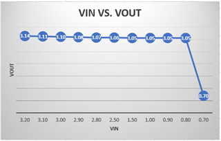
With my own testing done thus far, DC-wise, the part still operates within the operating range of the powered device. And with 3.2Vin, the part regulates down to about 3.15Vout and then regulates to 3.0V as the batteries continue to drain below 3.0V. See graph.
Is there any concern of the part becoming wildly unstable when Vin > Vout for a short while? or is it only a ripple concern. We will never have an input voltage as high as indicated on the forum.
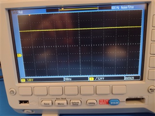
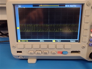
Here are images of the boost chip output DC and AC ripple with the boost converter tested with batteries and an open circuit voltage of 2.997VDC.
Would you mind please rerunning the test when the power supply is set to 3.2V and with short power supply leads? Please send me images of the AC ripple. If you can use a short ground lead on the scope, that would be preferred if possible.
Thank you!
Jeff


