HI Team,
Vin,Vout =3.3V
Load current=1A
PFA schematics.
How much is the output capacitance to be used?
Kindly revert.
Thanks,
Vidhya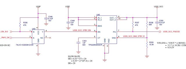
Original question:

HI Team,
Vin,Vout =3.3V
Load current=1A
PFA schematics.
How much is the output capacitance to be used?
Kindly revert.
Thanks,
Vidhya