


Other Parts Discussed in Thread: LM5145
Hello TI team,
- We just want to verify the component placement in our PCB for TPS Crank Simulator unit.
We have 4 layers in our PCB
- Layer-1 Top layer (Signal)
- Layer-2 Power 3.3V
- Layer-3 GND
- Layer-4 Bottom Layer (Signal)
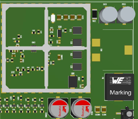
The below image from our PCB represent the DC-DC convertion components location by using the TPS40170 IC.
We have attached the PCB output files in PDF & Gerber files. We would like to know all the parameters are followed interms of component placement.
We are expecting the feedback from TI for the below
- Do we need any modification in component placement.
- TPS40170, Filter capacitors and Mosfets are placed in EMC Shield, Please cofirm us those components placed inside the shiled is right or wrong.
- Based on the TI confirmation we shall proceed the manufacturing of this board.
Please Let us know if more details required.
Regards,
Anbarasan M


