This thread has been locked.

If you have a related question, please click the "Ask a related question" button in the top right corner. The newly created question will be automatically linked to this question.

UCC28950: The OUT_C and OUT_D of UCC28590 outputs an abnormal waveform.

Part Number: UCC28950
Other Parts Discussed in Thread: UCC28951

Hi, E2E.

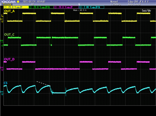
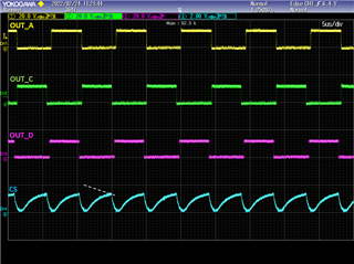
When the current limit works near the maximum duty, the OUT_C and OUT_D of UCC28950 outputs an abnormal waveform.

Can you tell me how to improve this abnormal operation?

DESCRIPTION

OUT_C becomes LOW due to the current limit, but after that (after about 20 ns), it returns to HIGH again for about 500 ns.

As a result, OUT_C turns on longer than usual.

During the next period, OUT_D should be HIGH, but OUT_D remains LOW and the OUTC side becomes HIGH.

Therefore, OUT_C and OUT_D, which should operate alternately, have abnormal outputs.

At this time, OUT_E and OUT_F synchronized with OUT_C and OUT_D also have abnormal outputs.

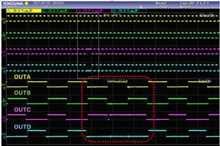
The OUT_A and OUT_B that synchronize with SYNC are normal.

In a more overloaded condition, the current limit completely limits the duty and returns to normal operation.

By lowering the current limit value or lowering the output voltage set value, it has been confirmed that abnormal operation disappears when the current limit is detected during duty control.

This phenomenon seems to occur when the current limit is detected near the maximum duty.

Regards,

Shimamura.

  • Hello Mike,

    Thank you for the linked information.

    I checked the contents of the link.

    However, I think that phenomenon is different from ours.

    It is that the current limit of the CS terminal is erroneously detected by noise due to the conduction current to the secondary side starting from the High of OUT_B (OUT_A).

    OUT_C, which is set to High before OUT_B’s, is Low condition due to a false detection of the current limit when OUT_B is High.

    Therefore, the High period of OUT_C is short and the High period of OUT_D is long.


    If this is the case of OUT_A instead of OUT_B, I think OUT_D High will be short and OUT_C High will be long.

    However, in our phenomenon, High of OUT_D is not shortened but completely disappears.

    The problem of the link destination occurs at that time OUT_A or OUT_B becomes High.

    On the other hand, our problem occurs after the current limit is detected correctly and OUT_C goes Low (about 20ns).

    This is the waveform at the time of abnormality including the waveform of the CS terminal.

    We have enough noise filters in the CS terminals.

    The current limit detection point is not 2V because overcurrent detection has slope compensation.

    The current limit detection can be imagined as having slope compensation like the white dotted line.

    Our phenomenon accurately detects the current limit near the maximum duty.

    When the current limit is detected, OUT_C goes Low once, but it goes High again after about 20ns.

    After that, OUT_D does not go High, but OUT_C goes High.

    During this period, the continuity to the secondary side is lost, and the voltage of the CS terminal also disappears.

    This is a waveform with a further increased output current.

    Since the current limit is detected in each cycle before the maximum control, OUT_D (OUT_C) goes High before OUT_A (OUT_B) and operates normally.


    I have checked similar topics as much as possible.

    I found a phenomenon in it that was the same as ours.


    https://e2e.ti.com/support/power-management-group/power-management/f/power-management-forum/857083/ucc28950-ucc28950-urgent-question-about-in-the-waveform-between-outc-and-outd


    Is there a way to improve the UCC28950 without changing it?


    Regards,

    Shimamura.

  • Hello,

    It is the same issue.  You can see that zero current is being demanded when C is shifted 180 degrees.

    Regards,

  • Hello Mike,

    Do you have any measures for solving that issue?
    Our CS terminal voltage is very clean.
    We don’t understand why zero current is being demanded.

    We recognize that it is necessary to detect the current for each pulse because of the current limit is a pulse-by-pulse method.
    The correct operation for zero duty is that OUT_D (OUT_C), which was previously High, goes Low as soon as OUT_A (OUT_B) goes High.
    In our phenomenon, OUT_D is not High before OUT_A.

    Also, there is a minimum pulse in the feedback loop, so there is no zero duty.
    If you enter burst mode, all outputs will be Low.

    Regards,
    Shimamura.

  • Hello,

    It really is not an issue.  The device at that point is trying to demand 0% duty cycle. 

    You might check your voltage amplifier output to make sure it is clean.  Please note the comp output is noise sensitive.  Section 8.2.2.10.1 of the data sheet gives instructions no how to probe the comp pin.

    Your CS signal has a lot of filtering on it.  It is hard to tell if the current is going discontinues when C and D are trying to demand 0% duty cycle.  You should turn off the SR FETs before the converter goes into DCM mode if you have not done that.

    Another thing that may help is setting Rtimin as low as possible.

    Regards,

  • Hello, Mike,

    We have confirmed that there is no problem with them.

    We recognize that neither the CS signal nor the COMP output demands zero duty.

    Our phenomenon is different from the zero-duty waveform, because it is different from the zero-duty waveform of the link you showed.

    The phenomenon of the following link shown earlier is the same as us.

    https://e2e.ti.com/support/power-management-group/power-management/f/power-management-forum/857083/ucc28950-ucc28950-urgent-question-about-in-the-waveform-b​​etween- outc-and-outd

    If this is the cause, is there a way to improve without changing the UCC28950?

    Regards,

    Shimamura

  • Hello,

    Did you check the SS pin if that get pulls low it will dominate over the comp voltage.

    Thank you for pointing out that thread on the UCC28950 at duty cycles greater than 50%.  It is recommended that you use the UCC28951 if duty cycles are greater than 90%.  It appears that your controller is trying to achieve 90% in your application.  So changing to the UCC28951 is one option as you mentiong.

    If you want to stay with the same IC.  You could do this by changing your transformer turns ratio to less than 90% to see if the issue goes away.

    Regards,

  • Hello, Mike.

    We have already confirmed that there is no problem with the SS pin.

    We described in the first inquiry:

    By lowering the current limit value or lowering the output voltage set value, it has been confirmed that abnormal operation disappears when the current limit is detected during duty control.

    This phenomenon seems to occur when the current limit is detected near the maximum duty.


    These show that a winding ratio of less than 90% solves the problem.

    However, we want a design with a duty of 90% or higher to make the output inductor very small.


    Q1.

     Is there a way to design the same IC with a duty of 90% or more?


    Q2.

    What logic problem in the IC causes this phenomenon?


    We will try to find a solution by knowing what is happening in the IC.

    Regards,

    Shimamura

  • Hello,

    1. The UCC28951 was designed to achieve greater than 90% duty cycle.  I believe this is the issue Collin Gillmore addressed in his thread and suggested using the UCC28951 and it solved the issue.  The device is pin for pin compatible with the UCC28950.

    2. I believe the issue you are seeing is why Collin wrote the following application note on choosing between the UCC28950 and UCC28951.  I believe in the application note he mentions the issue your are seeing with the UCC28950. https://www.ti.com/lit/pdf/slua853

    Regards,

  • Hello, Mike.


    Thank you for the information of the application note.

    I requested samples of UCC28951.

    Once we have them, we will check if the problem is solved.


    Many power supplies design to give maximum duty when the input drops, giving priority to efficiency and size.

    We have a problem with the rated input, but I think many power supplies fall into this problem when the input drops.

    I think it should be described the contents of this application note in the datasheet.


    Regards,

    Shimamura.

  • Hello,

    e2e technical support does not have sample stock. Could you please visit ti.com to get your samples.

    Regards,