This thread has been locked.

If you have a related question, please click the "Ask a related question" button in the top right corner. The newly created question will be automatically linked to this question.

UCC256402: Feedback circuit design for FB pin

Part Number: UCC256402
Other Parts Discussed in Thread: TIDA-010080, UCC256403, ATL431

Hello,

I am designing an AC-DC LLC resonant converter circuit with Boost PFC input circuit with UCC256402ADDBR IC. DC-DC input is in half bridge LLC structure with min:300 V type:390 V max:410 V parameters. I'm aiming for 60 V as output voltage and 700 W as output power. I need to design a feedback circuit for the UCC256402ADDBR IC FB pin. However, I am struggling. However, I use the TIDA-010080 reference design and the UCC25640X design calculator. Can you help with this ? If you want more information about the design, I can share it.

Kind regards
Cihangir

  • Hi Cihangir,

    You can refer the following e2e post regarding the feedback design:

    (+) UCC256301: How to set optocoupler current in UCC2560X feedback chain. - Power management forum - Power management - TI E2E support forums

    This post explains where to place zero and pole for the type 2 compensator for UCC25630x (this applies to UCC25640x as well).

    Please let me know if you have any further questions.

    Regards

    Manikanta P

  • Hi Manikanta,

    Thank you for your response. It was informative.
    1) In the link you mentioned, it is said that the Ifb current can be 350 uA at 110 C for the calculation of the R23 resistor. Where did this maximum value come from? I am designing with ucc256403 integration. When I examined the datasheet, 91uA was specified for the Ifb maximum value. Where can I find the Ifb maximum value for this calculation.

    2) I mentioned above that I used the TIDA-010080 reference design. I have attached the feedback circuit used in this design. In the design, the output voltage is defined as a variable between 42-58 V. ATL431 is used as shunt regulator. The output voltage of this regulator is defined as 2.5-36V in the datasheet. Doesn't it create a problem for the feedback design as the system output is more than the maximum value that the regulator can provide?

    3) What is the purpose of using the D14 zener diode? Is it related to the fact that the output voltage I mentioned in the 2nd question exceeds the maximum output voltage of the shunt regulator? If so, what should be the voltage value for the voltage divider calculation to be used on the reference pin?

    4) In my design, the output voltage is aimed at a maximum of 65 V. In case I am using the ATL431, I am exceeding the output voltage range of the ATL431. How should I revise the feedback circuit design?

    Regards

    Cihangir

  • Hi Cihangir,

    Please find the responses below:

    1. The max IFB current for UCC256403 is 182uA. Please see the screen shot of the datasheet below.

    2,3 . You are correct. You can not exceed the maximum cathode to anode voltage of the regulator. That's the reason, Zener is used in this case. You need to design the resistor divider such that reference pin is at 2.5V for the given output voltage.

    In the reference design, variable resistor is used to adjust the output voltage. For example, assume variable resistor is lowest point in which case, 51k is shorted.

    In that case output voltage will be regulated at 58V (you can obtain this value by applying KCL at the ref pin.). As you change the variable resistor, the output voltage gets adjusted.

    (2.5V/9.1k)=(Vout-2.5V)/(75k+130k)  ==> Vout=58V

    4. You can use multiple zener voltages for the 65V output voltage. Please refer the following reference design.

    PMP40379 Schematic

    Please let me know if you have any further questions.

    Regards

    Manikanta P

  • Hello,

    After your last replies I calculated the upper resistor, feedback pull-up resistor, low resistor in the feedback circuit. The values ​​are calculated for the output voltage of 61V.  As a shunt zener, an element similar to ATL431 from a different manufacturer was used. The values ​​are as follows.

    Rupper=69kOhm

    Rf= 10kOhm

    Rlow=3kOhm

    R_FL=6.04Ohm

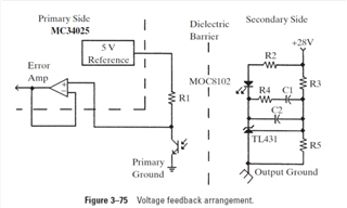
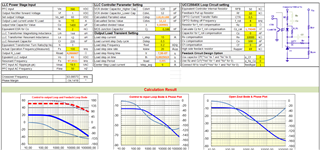
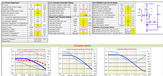
    I am using the UCC25640X design calculator for feedback compensation. I could not find a document directly explaining how to calculate Cv and Rv values ​​when I do not use Cf, Rz and Cz elements in the circuit in the attached image.

    However, I do know the following about Bode curves.

    1) The phase difference should be a minimum of 45 degrees where the gain, ie 20log(Vout/Vin) equation is 0 dB and larger. But for more stable and robust feedback, it should be between 70 - 80. 0dB is when the vout and vin voltages are equal in the equation. There must be enough phase difference to avoid oscillation.

    2) The crossover frequency of the system should be chosen as high as possible. The crossover frequency is the frequency at which the gain reaches 0dB. Choosing this frequency high will speed up the system's response to transient response, that is, instantaneous, transient situations.

    4) When the phase curve is at 0 degrees, the gain should be at least 10 - 15dB.

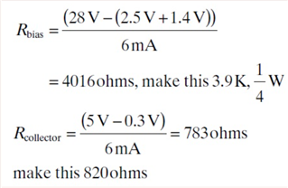
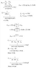
    Along with these rules, I found the following calculations related to the design similar to the subject in the book "Marty Brown's Power Supply CookBook".

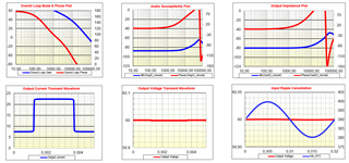
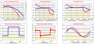
    When I try to make the output voltage waveform as flat as possible in the Output Voltage Transient Waveform graph in the calculator, the corssover frequency increases, but the Phase Margin falls below -45 degrees. As far as I understand, this does not comply with the rules I mentioned above.

    However, when I design by following the rules mentioned above and the formulas mentioned in the book, the waveform appears wavy. However, the pahse margin is +45 degrees and the crossover frequency is acceptably high.

    I think the best solution for this is to decide on the values ​​by testing. But I have no such opportunity.

    What do I need to do to get started and an acceptable optimal feedback optimization design of the circuit?

    Is there a validated design method for calculating Cv and Rv values? How necessary is the use of Cf, Rz and Cz elements? If necessary, how should it be calculated? I know it's a very detailed question, but different sources confuse me on this. Thank you for your interest. Kind regards Cihangir.

  • Hi Cihangir,

    Investigation_on_the_small_signal_characteristic_based_on_the_LLC_hybrid_hysteretic_charge_control.pdf

    This document derives the transfer function of type 2 compensator. Same document has been used for the design calculator. I would recommend you to go through controller part of this paper.

    For HHC control, type 2 controller is sufficient (similar to current mode control). If you would like to increase the cross over frequency, you would need to add Cf,Rz,Cz elements. 

    So for converter startup you can just add type two compensator. 

    following e2e post explains where to place poles and zeroes for type 2 compensator.

    UCC256301: How to set optocoupler current in UCC2560X feedback chain. - Power management forum - Power management - TI E2E support forums

    Please send me a direct message through e2e. I can share some more documents regarding this topic.

    Regards

    Manikanta P